Basic Introduction to Microprocessor, Microcomputer, Microcontroller
A microprocessor is a small electronic chip that processes data and performs tasks in a computer. It is also called a processor or CPU (Central Processing Unit).
Building Blocks of microprocessor:

Components of microprocessor:
A microprocessor has three main parts
1.Arithmetic Logic Unit (ALU): It does math calculations (Sum, Subtract etc) and logical decisions (and , or etc) using data from input devices or memory.
2.Control Unit (CU): It directs the flow of data and instructions inside the microprocessor.
3.Register Array: A group of small, fast storage units that temporarily hold data and instructions while the microprocessor works.
একটি মাইক্রোপ্রসেসর হলো একটি ছোট ইলেকট্রনিক চিপ(chip) যা একটি কম্পিউটারে ডেটা প্রসেস করে এবং বিভিন্ন কাজ সম্পন্ন করে। একে প্রসেসর বা সিপিইউ (CPU – Central Processing Unit)-ও বলা হয়।
মাইক্রোপ্রসেসরের প্রধান অংশ (Building Blocks of microprocessor)

একটি মাইক্রোপ্রসেসরের তিনটি প্রধান অংশ রয়েছে:
১. ALU – Arithmetic Logic Unit): এটি ইনপুট ডিভাইস বা মেমরি থেকে ডেটা ব্যবহার করে গাণিতিক গণনা (যোগ, বিয়োগ ইত্যাদি) এবং লজিক্যাল (and, or operation) সিদ্ধান্ত নেয়।
২. (CU – Control Unit): এটি মাইক্রোপ্রসেসরের অভ্যন্তরে ডেটা এবং নির্দেশাবলীর(instruction) প্রবাহকে (flow) পরিচালনা করে।
৩. (Register Array): এটি ছোট, দ্রুত স্টোরেজ ইউনিটের একটি গ্রুপ, যা মাইক্রোপ্রসেসর কাজ করার সময় অস্থায়ীভাবে ডেটা এবং নির্দেশাবলী (instruction) ধারণ করে।
A microcomputer is a small, complete computer system built around a microprocessor. It has a CPU (microprocessor), memory, input/output devices (like keyboard and monitor), and storage.
Building Blocks of microcomputer:

Components of Microcomputer:
1.Central Processing Unit (CPU): The brain of the computer that processes instructions and controls other parts.
2.Memory: Stores data and programs temporarily (RAM) or permanently (hard drive/SSD).
3.Input Devices: Tools like a keyboard and mouse that allow users to enter data.
4.Output Devices: Devices like monitors and printers that display or produce the results of processing.
একটি মাইক্রোকম্পিউটার হলো একটি ছোট, সম্পূর্ণ কম্পিউটার সিস্টেম যা একটি মাইক্রোপ্রসেসরের ওপর ভিত্তি করে তৈরি করা হয়। এতে একটি সিপিইউ (CPU) (মাইক্রোপ্রসেসর), মেমরি, ইনপুট/আউটপুট ডিভাইস (যেমন কিবোর্ড ও মনিটর) এবং স্টোরেজ থাকে।
মাইক্রোকম্পিউটারের প্রধান অংশ (Building Blocks of Microcomputer)

একটি মাইক্রোকম্পিউটারের প্রধান অংশগুলো হলো:
১. সেন্ট্রাল প্রসেসিং ইউনিট (CPU): এটি কম্পিউটারের মস্তিষ্ক, যা নির্দেশাবলী প্রসেস করে এবং অন্যান্য অংশকে নিয়ন্ত্রণ করে।
২. মেমরি (Memory): এটি ডেটা এবং প্রোগ্রাম সাময়িকভাবে (RAM) অথবা স্থায়ীভাবে (হার্ড ড্রাইভ/SSD) সংরক্ষণ করে।
৩. ইনপুট ডিভাইস (Input Devices): কিবোর্ড ও মাউসের মতো টুলস, যা ব্যবহারকারীদের ডেটা ইনপুট করার সুযোগ দেয়।
৪. আউটপুট ডিভাইস (Output Devices): মনিটর ও প্রিন্টারের মতো ডিভাইস, যা প্রসেসিং-এর ফলাফল প্রদর্শন বা তৈরি করে।
A microcontroller is a complete computing system fully implemented on a single chip. It includes a microprocessor (CPU), memory (RAM and ROM), and input/output peripherals all integrated together.

Uses of Microcontroller:
- Home Appliances: Controls washing machines, microwave ovens, air conditioners, etc.
- Automobiles: Manages engine control, airbag systems, ABS, and other car electronics.
- Consumer Electronics: Found in remote controls, cameras, and gaming consoles.
- Industrial Automation: Controls machines, robots, and assembly lines.
- Medical Devices: Used in heart rate monitors, blood pressure devices, and other medical instruments.
- Embedded Systems: Powers smart devices like IoT gadgets, smart meters, and wearables.
একটি মাইক্রোকন্ট্রোলার হলো একটি সম্পূর্ণ কম্পিউটিং সিস্টেম যা একটি মাত্র চিপে পুরোপুরি বাস্তবায়িত হয়। এতে একটি মাইক্রোপ্রসেসর (CPU), মেমরি (RAM এবং ROM), এবং ইনপুট/আউটপুট পেরিফেরালস সবই একসাথে সমন্বিত থাকে।

মাইক্রোকন্ট্রোলারের ব্যবহার (Uses of Microcontroller)
- গৃহস্থালী সরঞ্জাম (Home Appliances): ওয়াশিং মেশিন, মাইক্রোওয়েভ ওভেন, এয়ার কন্ডিশনার ইত্যাদি নিয়ন্ত্রণ করে।
- অটোমোবাইলস (Automobiles): ইঞ্জিনের নিয়ন্ত্রণ, এয়ারব্যাগ সিস্টেম, ABS এবং অন্যান্য গাড়ির ইলেকট্রনিক্স পরিচালনা করে।
- কনজিউমার ইলেকট্রনিক্স (Consumer Electronics): রিমোট কন্ট্রোল, ক্যামেরা এবং গেমিং কনসোলে পাওয়া যায়।
- শিল্পে অটোমেশন (Industrial Automation): মেশিন, রোবট এবং অ্যাসেম্বলি লাইন নিয়ন্ত্রণ করে।5
- চিকিৎসা সরঞ্জাম (Medical Devices): হার্ট রেট মনিটর, ব্লাড প্রেসার ডিভাইস এবং অন্যান্য চিকিৎসা যন্ত্রপাতিতে ব্যবহৃত হয়।
- এমবেডেড সিস্টেম (Embedded Systems): আইওটি গ্যাজেট, স্মার্ট মিটার এবং পরিধানযোগ্য (wearables) ডিভাইসের মতো স্মার্ট ডিভাইসগুলোকে শক্তি জোগায়।
- Intel 4004: 4-bit processor, 2300 transistors, 740 kHz clock speed. It could process 4 bits of data at once.
- Intel 8008: 8-bit processor introduced in 1972. It laid the foundation for early personal computers like the Altair 8800.
- Intel 8085: Clock speed of 3 to 5 MHz, required fewer external components due to better integration.
- Zilog Z80: Popular in early home computers, backward compatible with Intel 8080 software.
- Intel 8086: 16-bit processor with 5 to 10 MHz clock speed. Used segmented memory addressing to support larger programs.
- Motorola 68000: Clock speed of 4 to 16.67 MHz, special instructions for BCD arithmetic. Used in Unix workstations and Apple MacOS systems.
- Intel 80386: First full 32-bit x86 processor. Supported modern operating systems, virtual memory, and multitasking.
- PowerPC Processor: Developed by Apple-IBM-Motorola (AIM) for high-performance and energy-efficient computing.
- Intel Pentium 4: 32-bit processor with clock speed over 3 GHz, paving the path of modern computing.
- AMD x86-64 Architecture: Supports both 32-bit and 64-bit applications.
- Multi-core functionality up to 64 cores for better performance and multitasking.
- Integrated graphics support for gaming, video editing, and robotics.
- Higher energy efficiency compared to earlier g

- Intel 4004: 4-bit processor, 2300 transistors, 740 kHz clock speed। একসাথে 4 bits data process করতে পারত।
- Intel 8008: 1972-এ introduced 8-bit processor। এটি early personal computers যেমন Altair 8800-এর foundation তৈরি করেছিল।
- Intel 8085: 3 থেকে 5 MHz clock speed, better integration-এর কারণে কম external components প্রয়োজন ছিল।
- Zilog Z80: Early home computers-এ popular, Intel 8080 software-এর সাথে backward compatible ছিল।
- Intel 8086: 16-bit processor 5 থেকে 10 MHz clock speed-সহ। Larger programs support করতে segmented memory addressing ব্যবহার করত।
- Motorola 68000: 4 থেকে 16.67 MHz clock speed, BCD arithmetic-এর জন্য special instructions। Unix workstations এবং Apple MacOS systems-এ ব্যবহৃত হতো।
- Intel 80386: প্রথম full 32-bit x86 processor। Modern operating systems, virtual memory, এবং multitasking support করত।
- PowerPC Processor: Apple-IBM-Motorola (AIM) দ্বারা developed, high-performance এবং energy-efficient computing-এর জন্য।
- Intel Pentium 4: 32-bit processor 3 GHz-এর বেশি clock speed-সহ, modern computing-এর path pave করেছিল।
- AMD x86-64 Architecture: 32-bit এবং 64-bit applications উভয় support করে।
- 64 cores পর্যন্ত multi-core functionality better performance এবং multitasking-এর জন্য।
- Gaming, video editing, এবং robotics-এর জন্য integrated graphics support।
- আগের generations-এর তুলনায় বেশি energy efficiency।

A microprocessor is a compact integrated circuit that serves as the central processing unit of a computer. It performs arithmetic, logic, and control operations based on instructions from software programs. Below are the key features that make microprocessors essential in modern computing.
1. Cost-effective
Microprocessor chips are mass-produced using semiconductor fabrication techniques, making them available at very low prices. A single chip replaces hundreds of discrete components like transistors, resistors, and capacitors. This reduces the overall cost of building computers, smartphones, and embedded systems.
Example: A modern ARM processor costing a few dollars can power an entire smartphone.
2. Small Size
A microprocessor is manufactured on a tiny silicon chip, often just a few square millimeters. This small size makes it highly portable and allows manufacturers to build compact devices like laptops, tablets, and wearable technology.
Example: The Intel Core i7 processor fits in the palm of a hand yet performs billions of calculations per second.
3. Low Power Consumption
Microprocessors are built using Metal-Oxide Semiconductor (MOS) technology, which requires very little electrical power to operate. Low power consumption means less heat generation, longer battery life for mobile devices, and reduced cooling costs for data centers.
Example: Smartphone processors run for a full day on a small battery because they consume only a few watts.
4. Versatility
The same microprocessor hardware can be used in countless applications simply by changing the software program it runs. One chip can power a washing machine, a medical scanner, or a gaming console depending on the loaded software.
Example: The ARM architecture appears in cars, TVs, phones, and servers because software configures it for each task.
5. Reliability
Since a microprocessor is a single integrated circuit, it has very few physical connections that can fail. The failure rate of IC-based microprocessors is extremely low compared to systems built from many separate components. This makes them dependable for critical applications.
Example: Aircraft control systems and medical devices use microprocessors because they rarely malfunction under stress.
Microprocessor হলো একটি compact integrated circuit যা computer-এর central processing unit হিসেবে কাজ করে। এটি software programs থেকে instructions-এর উপর ভিত্তি করে arithmetic, logic, এবং control operations perform করে। নিচে সেই key features দেওয়া হয়েছে যা microprocessors-কে modern computing-এ essential করে তোলে।<
1. Cost-effective
Microprocessor chips semiconductor fabrication techniques ব্যবহার করে mass-produced হয়, যা তাদের খুব কম দামে available করে। একটি single chip transistors, resistors, এবং capacitors এর মতো hundreds of discrete components replace করে। এটি computers, smartphones, এবং embedded systems তৈরির overall cost কমায়।
Example: কয়েক ডলার দামের একটি modern ARM processor পুরো smartphone power করতে পারে।
2. Small Size
Microprocessor কয়েক square millimeters-এর ছোট silicon chip-এ manufacture করা হয়। এই ছোট size এটিকে highly portable করে এবং manufacturers-কে laptops, tablets, এবং wearable technology এর মতো compact devices তৈরি করতে দেয়।
Example: Intel Core i7 processor হাতের তালুতে ফিট করে কিন্তু প্রতি second-এ billions of calculations perform করে।
3. Low Power Consumption
Microprocessors Metal-Oxide Semiconductor (MOS) technology ব্যবহার করে তৈরি করা হয়, যা operate করতে খুব কম electrical power প্রয়োজন। Low power consumption মানে কম heat generation, mobile devices-এর জন্য longer battery life, এবং data centers-এর জন্য reduced cooling costs।
Example: Smartphone processors ছোট battery-এ পুরো দিন চলে কারণ এরা মাত্র কয়েক watts consume করে।
4. Versatility
একই microprocessor hardware countless applications-এ ব্যবহার করা যায় শুধু software program change করেই। একটি chip washing machine, medical scanner, বা gaming console power করতে পারে loaded software-এর উপর নির্ভর করে।
Example: ARM architecture cars, TVs, phones, এবং servers-এ দেখা যায় কারণ software এটিকে প্রতিটি task-এর জন্য configure করে।
5. Reliability
Microprocessor একটি single integrated circuit হওয়ায় এর খুব কম physical connections fail করতে পারে। IC-based microprocessors-এর failure rate many separate components দিয়ে তৈরি systems-এর তুলনায় extremely low। এটি critical applications-এর জন্য dependable করে তোলে।
Example: Aircraft control systems এবং medical devices microprocessors ব্যবহার করে কারণ এরা stress-এর অধীনে rarely malfunction করে।
A microprocessor is the central brain of a computer system that performs multiple essential functions to process data and control operations. Below are the major functions explained with examples.
1. Arithmetic Operations
Arithmetic operations are the most basic function of a microprocessor. It performs calculations like addition, subtraction, multiplication, and division. These operations are critical for tasks such as solving math problems, rendering graphics, and processing financial data.
Examples:
- Calculating the total of a list of numbers in a spreadsheet.
- Measuring distances in a GPS-based navigation system.
- Calculating interest rates in banking software.
2. Logical Operations
Logical operations allow the microprocessor to compare values and make decisions based on conditions. These operations use logic gates to evaluate true or false states.
Examples:
- Verifying if a password matches during user login.
- Sorting a list of items based on price, date, or name.
- Filtering emails as read, unread, spam, or important based on keywords.
3. Data Handling
Data handling involves moving, storing, and retrieving data between different parts of the system. The microprocessor manages how data flows between memory, storage, and external devices.
Examples:
- Fetching a webpage from a remote server to display in a browser.
- Saving a document, PDF, or image file to the hard disk.
- Copying photos or videos from a computer to a USB pen drive.
4. Control Operations
Control operations manage the sequence and flow of instructions. The microprocessor decides the order in which tasks are executed and coordinates other hardware components.
Examples:
- Adjusting the speed of a laptop cooling fan based on internal temperature.
- Regulating cooking time and temperature in a microwave oven.
- Controlling traffic light sequences based on real-time traffic density.
5. Instruction Execution
Instruction execution is the core function where the microprocessor reads, decodes, and carries out program instructions step by step. Every software action is broken down into simple instructions that the processor executes.
Examples:
- Opening Microsoft Word when the user clicks the icon.
- Removing the background from an image in photo editing software.
- Running a full system scan using antivirus software.
6. Interrupt Handling
Interrupt handling allows the microprocessor to pause current tasks and respond to urgent events. It ensures that high-priority actions are addressed immediately without waiting for ongoing processes to finish.
Examples:
- Pausing a video playback when the battery level drops critically low.
- Displaying a pop-up notification when a new message arrives.
- Stopping the printer immediately when the user presses the cancel button.
7. Power Management
Power management helps the microprocessor control energy consumption by putting unused components into low-power states. This extends battery life and reduces heat generation.
Examples:
- Reducing processor and memory power when the computer is idle.
- Turning off screen backlight after a period of inactivity.
- Slowing down the cooling fan when the device temperature is normal.
Microprocessor হলো computer system-এর central brain যা data process এবং operations control করতে multiple essential functions perform করে। নিচে major functions examples সহ ব্যাখ্যা করা হয়েছে।
1. Arithmetic Operations
Arithmetic operations microprocessor-এর সবচেয়ে basic function। এটি addition, subtraction, multiplication, এবং division এর মতো calculations perform করে। এই operations math problems solve করা, graphics render করা, এবং financial data process করার জন্য critical।
Examples:
- Spreadsheet-এ numbers-এর total calculate করা।
- GPS-based navigation system-এ distances measure করা।
- Banking software-এ interest rates calculate করা।
2. Logical Operations
Logical operations microprocessor-কে values compare করতে এবং conditions-এর উপর ভিত্তি করে decisions নিতে দেয়। এই operations logic gates ব্যবহার করে true বা false states evaluate করে।
Examples:
- User login-এর সময় password match verify করা।
- Price, date, বা name-এর উপর ভিত্তি করে items sort করা।
- Keywords-এর উপর ভিত্তি করে emails read, unread, spam, বা important হিসেবে filter করা।
3. Data Handling
Data handling data move, store, এবং retrieve করাকে involve করে system-এর বিভিন্ন অংশের মধ্যে। Microprocessor memory, storage, এবং external devices-এর মধ্যে data flow manage করে।
Examples:
- Browser-এ display করতে remote server থেকে webpage fetch করা।
- Hard disk-এ document, PDF, বা image file save করা।
- Computer থেকে USB pen drive-এ photos বা videos copy করা।
4. Control Operations
Control operations instructions-এর sequence এবং flow manage করে। Microprocessor কোন order-এ tasks execute হবে তা decide করে এবং অন্য hardware components coordinate করে।
Examples:
- Internal temperature-এর উপর ভিত্তি করে laptop cooling fan-এর speed adjust করা।
- Microwave oven-এ cooking time এবং temperature regulate করা।
- Real-time traffic density-এর উপর ভিত্তি করে traffic light sequences control করা।
5. Instruction Execution
Instruction execution core function যেখানে microprocessor program instructions step by step read, decode, এবং carry out করে। প্রতিটি software action simple instructions-এ break down হয় যা processor execute করে।<
Examples:
- User icon click করলে Microsoft Word open করা।
- Photo editing software-এ image-এর background remove করা।
- Antivirus software ব্যবহার করে full system scan run করা।
6. Interrupt Handling
Interrupt handling microprocessor-কে current tasks pause করে urgent events-এ respond করতে দেয়। এটি ensure করে যে high-priority actions immediately address হয় ongoing processes শেষ হওয়ার অপেক্ষা না করে।<
Examples:
- Battery level critically low হলে video playback pause করা।
- New message arrive করলে pop-up notification display করা।
- User cancel button press করলে immediately printer stop করা।
7. Power Management
Power management microprocessor-কে energy consumption control করতে সাহায্য করে unused components-কে low-power states-এ রেখে। এটি battery life extend করে এবং heat generation কমায়।<
Examples:
- Computer idle থাকলে processor এবং memory power reduce করা।
- নির্দিষ্ট সময় inactivity থাকলে screen backlight turn off করা।
- Device temperature normal থাকলে cooling fan speed slow করা।
Processor and Categories of Microproecessor (CISC & RISC)
Processor (CPU – Central Processing Unit)
The Processor is often called the brain of the computer because it is responsible for executing instructions and processing data.
Working Principle of CPU
A processor takes instructions and data as inputs.
- The instructions tell the processor what operation needs to be performed on the data.
- The data is then manipulated or processed according to those instructions.
Each processor has its own Instruction Set – This is nothing but a collection of instructions or operations that the processor understands and can execute.
প্রসেসরকে কম্পিউটারের মস্তিষ্ক বলা হয়, কারণ এটি নির্দেশাবলী (instruction) execute করা এবং ডেটা প্রসেসিং করার জন্য দায়ী।
সিপিইউ-এর কার্যপ্রণালী (Working Principle of CPU)
একটি প্রসেসর ইনপুট হিসেবে নির্দেশাবলী (instructions) এবং ডেটা (data) গ্রহণ করে।
Instruction প্রসেসরকে জানায় যে ডেটার ওপর কী ধরনের অপারেশন সম্পন্ন করতে হবে।
এরপর এই ডেটা নির্দেশাবলী (instruction) অনুযায়ী পরিবর্তিত বা প্রসেস হয়।
প্রতিটি প্রসেসরের নিজস্ব ইনস্ট্রাকশন সেট (Instruction Set) রয়েছে যা হলো একগুচ্ছ নির্দেশাবলী বা অপারেশনের সমষ্টি, যা প্রসেসর বুঝতে এবং execute করতে পারে।
Computer architecture can be classified into two major types based on instruction set This is nothing but a collection of instructions or operations that the processor understands and can execute.
- CISC – Complex Instruction Set Computer
- RISC – Reduced Instruction Set Computer
But before we look at these terms, let’s go back in time to understand why these two architectures were formed in the first place.
Background (Before 1970s)
- Memory (RAM) was slow and expensive.
- Programs were usually written in high-level languages (HLLs) because they were more user-friendly.
- The job of the compiler was to convert these HLL instructions into machine-level instructions so that the processor could execute them.
As high-level languages became more complex, designing compilers became difficult, error-prone, and time-consuming. To make things easier, computer architects wanted to bridge the gap between high-level language code and machine instructions.
Birth of CISC (Complex Instruction Set Computer)
The solution was to have compact, powerful instructions that could do more work with a single command.
CISC Instruction Example
MULT 1:2, 2:3
This single, compact instruction does multiple tasks internally:
- Fetch: Fetches data from memory locations 1:2 and 2:3.
- Load to Registers:
- Register A ← 2
- Register B ← 3
- Multiply: Performs A × B → 2 × 3 = 6
- Store: Stores result back into the appropriate memory location.
Observation
- One single instruction (MULT 1:2, 2:3) performs all four steps.
- Compact code → fewer instructions per program.
- But hardware must be complex to handle all these tasks internally.
This made programming easier and reduced the number of instructions in a program.
But there was a trade-off:
- The hardware became more complex because it had to support all these advanced instructions.
- More transistors were needed → resulting in larger, more expensive processors.
- Higher complexity → increased power consumption and heat dissipation.
Important Note: Computer architects did not intentionally create CISC. It was a natural evolution of processor design based on the needs of that time.
কম্পিউটার আর্কিটেকচারকে ইনস্ট্রাকশন সেট-এর ওপর ভিত্তি করে দুটি প্রধান ভাগে ভাগ করা যায়। ইনস্ট্রাকশন সেট হলো একগুচ্ছ নির্দেশ বা অপারেশনের সমষ্টি যা একটি প্রসেসর বুঝতে ও execute করতে পারে। এই দুটি ভাগ হলো:
- CISC – Complex Instruction Set Computer
- RISC – Reduced Instruction Set Computer
এই দুটি আর্কিটেকচার কেন তৈরি হয়েছিল, তা বুঝতে হলে আমাদের সময়ের পেছনে যেতে হবে।
(Background (Before 1970s))
- মেমরি (RAM) তখন ছিল ধীরগতির এবং ব্যয়বহুল।
- প্রোগ্রামগুলো সাধারণত হাই-লেভেল ল্যাঙ্গুয়েজেস (HLLs) লেখা হতো, কারণ এগুলো ব্যবহারকারীদের জন্য বেশি সহজ ছিল।
- কম্পাইলারের কাজ ছিল এই HLL নির্দেশগুলোকে মেশিন-লেভেল নির্দেশাবলীতে রূপান্তর করা, যাতে প্রসেসর সেগুলো execute করতে পারে।
- হাই-লেভেল ল্যাঙ্গুয়েজগুলো আরও জটিল হয়ে ওঠায়, কম্পাইলার ডিজাইন করা কঠিন, ত্রুটিপূর্ণ এবং সময়সাপেক্ষ হয়ে দাঁড়ায়।
বিষয়টি সহজ করার জন্য, কম্পিউটার স্থপতিরা হাই-লেভেল ল্যাঙ্গুয়েজ কোড এবং মেশিন নির্দেশাবলীর মধ্যেকার গ্যাপ কমাতে চেয়েছিলেন।
CISC-এর জন্ম (Birth of CISC)
এর সমাধান ছিল এমন কিছু কমপ্যাক্ট এবং শক্তিশালী নির্দেশ(instruction) তৈরি করা, যা একটি একক কমান্ড দিয়ে অনেকগুলো কাজ করতে পারে।
CISC ইনস্ট্রাকশনের উদাহরণ
CISC Instruction Example
MULT 1:2, 2:3
এই একটি মাত্র কমপ্যাক্ট ইনস্ট্রাকশন অভ্যন্তরীণভাবে একাধিক কাজ সম্পন্ন করে:
- Fetch: মেমরি লোকেশন 1:2 এবং 2:3 থেকে ডেটা নিয়ে আসে।
- Load to Registers:
- রেজিস্টার A ← 2
- রেজিস্টার B ← 3
- Multiply: A × B → 2 × 3 = 6 সম্পন্ন করে।
- Store: ফলাফলটি উপযুক্ত মেমরি লোকেশনে আবার সংরক্ষণ করে।
পর্যবেক্ষণ (Observation)
- একটি একক ইনস্ট্রাকশন (MULT 1:2, 2:3) সমস্ত চারটি ধাপ সম্পন্ন করে।
- কিন্তু এই সব কাজ অভ্যন্তরীণভাবে সামলানোর জন্য হার্ডওয়্যার আরো জটিল(Complex) হয়ে যায়।
- এই পদ্ধতিটি প্রোগ্রামিংকে সহজ করে তুলেছিল এবং প্রোগ্রামের মধ্যেকার নির্দেশাবলীর সংখ্যা কমিয়ে এনেছিল।
কিন্তু এর একটি বড় সীমাবদ্ধতা ছিল:
- হার্ডওয়্যার আরও জটিল (Complex) হয়ে যায়, কারণ তাকে এই সব উন্নত নির্দেশাবলী(instruction) execute করতে হতো।
- যার ফলে আরও বেশি ট্রানজিস্টর প্রয়োজন হয়, এজন্য প্রসেসরগুলো বড় এবং ব্যয়বহুল হয়ে ওঠে।
- ফলশ্রুতিতে বিদ্যুৎ খরচ এবং তাপ নির্গমনও বেড়ে যায়।
Important Note:
কম্পিউটার স্থপতিরা ইচ্ছাকৃতভাবে CISC তৈরি করেননি। এটি ছিল সেই সময়ের প্রয়োজন অনুযায়ী প্রসেসর ডিজাইনের একটি স্বাভাবিক বিবর্তন।
Birth of RISC (Reduced Instruction Set Computer) – Early 1980s
In the 1980s, researchers discovered something interesting: Only 20% of instructions were used 80% of the time in programs. This meant many of the complex CISC instructions were rarely used.
This led to a new idea:
- Create a smaller, simpler instruction set that contains only the most commonly used operations.
- Let the compiler handle more work by combining these simple instructions when needed.
RISC architecture focuses on a small set of simple instructions that can be executed very quickly, usually in a single clock cycle.
Thus, RISC architecture was born.
RISC Instruction Example
Load A, 1:2
Load B, 2:1
Prod A, B
Store 1:2, A

Step-by-Step Execution:
- Load A, 1:2 → Loads data from memory location 1:2 into Register A.
- Load B, 2:1 → Loads data from memory location 2:1 into Register B.
- Prod A, B → Multiplies A and B, result stored back in A.
- Store 1:2, A → Stores result from A back into memory location 1:2.
Observation:
- Simple step-by-step execution
- Requires multiple instructions (more memory)
- But each instruction is fast and takes one clock cycle
RISC (Reduced Instruction Set Computer)-এর জন্ম – ১৯৮০ এর দশকের শুরুতে
১৯৮০-এর দশকে গবেষকরা একটি গুরুত্বপূর্ণ বিষয় লক্ষ্য করলেন:
প্রোগ্রামে ব্যবহৃত instruction এর মধ্যে মাত্র ২০% instruction ৮০% সময় ব্যবহার হয়। এতে দেখা গেলো, অনেক জটিল CISC instruction খুবই কম ব্যবহৃত হয়।
এরপর একটি নতুন ধারণার তৈরি হলো আর তা হলঃ একটি ছোট, সহজ instruction set তৈরি করা যেখানে শুধুমাত্র সবচেয়ে বেশি ব্যবহৃত অপারেশন বা Instruction গুলো থাকবে।
প্রয়োজন হলে কম্পাইলারকে বেশি কাজ করতে দেওয়া হবে যাতে সে সহজ instruction গুলো মিলিয়ে জটিল কাজ সম্পাদন করতে পারে। RISC architecture মূলত ছোট সেটের সহজ instruction ব্যবহার করে যেগুলো খুব দ্রুত (সাধারণত একটি clock cycle-এর মধ্যে) এক্সিকিউট করা যায়।
এইভাবে RISC architecture-এর জন্ম হয়।
RISC Instruction Example
Load A, 1:2
Load B, 2:1
Prod A, B
Store 1:2, A

(Step-by-Step Execution)
- Load A, 1:2 → মেমরি লোকেশন 1:2 থেকে ডেটা রেজিস্টার A-তে লোড করে।
- Load B, 2:1 → মেমরি লোকেশন 2:1 থেকে ডেটা রেজিস্টার B-তে লোড করে।
- Prod A, B → A ও B-কে গুণ করে; গুনফল আবার রেজিস্টার A-তে সংরক্ষণ করা হয়।
- Store 1:2, A → রেজিস্টার A থেকে ফলাফল মেমরি লোকেশন 1:2-এ স্টোর করে।
RISC পদ্ধতিটি সহজ, ধাপে ধাপে কাজ করে। যদিও এর জন্য একাধিক নির্দেশাবলীর প্রয়োজন হয় (ফলে মেমরি বেশি লাগে), প্রতিটি নির্দেশই দ্রুত কাজ করে এবং সাধারণত একটি সিঙ্গেল ক্লক সাইকেলে সম্পন্ন হয়। এই ডিজাইন হার্ডওয়্যারকে আরও সহজ, দ্রুত এবং বিদ্যুৎ-সাশ্রয়ী করে তোলে।
System Bus : Address Bus, Data Bus, Control Bus
The System Bus is the communication pathway that connects the CPU, memory, and input/output devices. It is like the nerve system of a computer, carrying signals and data between components.
A System Bus is a collection of parallel wires or signal lines that connect the major components of a computer system and allow them to communicate.
Types Of Buses
There are three main types of buses in a computer system
- Address Bus
- Data Bus
- Control Bus
বাসের প্রকারভেদ (Types Of Buses)
একটি কম্পিউটার সিস্টেমে প্রধানত তিন ধরনের বাস থাকে:
- অ্যাড্রেস বাস (Address Bus)
- ডেটা বাস (Data Bus)
- কন্ট্রোল বাস (Control Bus)

The Address Bus is a collection of wires used to identify specific locations in memory. In other words, the information used to describe memory locations travels along the address bus.
Purpose
- The address bus transports memory addresses which the CPU wants to access in order to read or write data.
- It specifies the location in memory or the I/O device where the data is stored or needs to be stored.
Characteristics
1. Unidirectional:
- The address always flows from CPU → Memory/I/O devices.
- Memory or I/O devices cannot send addresses back to the CPU.
2. Determines Maximum Addressable Memory:
The number of lines (width) of the address bus determines how many unique memory locations can be addressed.
Example:
- 4-bit address bus → 2⁴ = 16 memory locations (16 Bytes)
- 16-bit address bus → 2¹⁶ = 65,536 memory locations (64 KB)
- 20-bit address bus → 2²⁰ = 1,048,576 memory locations (1 MB)
3. Generated By CPU: The CPU generates the address signals to tell memory or I/O which location to access.
অ্যাড্রেস বাস হলো তারের একটি সংগ্রহ, যা কম্পিউটারের মেমরি বা অন্য কোনো ডিভাইসের নির্দিষ্ট অবস্থান(location) চিহ্নিত করার জন্য ব্যবহৃত হয়। সহজ কথায়, এটি সেই রাস্তা (communication path) যার মাধ্যমে ডেটা কোথায় আছে বা কোথায় যাবে, সেই (address) সম্পর্কিত তথ্য আদান প্রদান করা হয়।
অ্যাড্রেস বাসের উদ্দেশ্য
অ্যাড্রেস বাসের প্রধান কাজ হলো সেইসব মেমরি অ্যাড্রেস পরিবহন করা, যা CPU কোনো ডেটা read বা write এর জন্য অ্যাক্সেস করতে চায়।
বৈশিষ্ট্য
১. একমুখী (Unidirectional): অ্যাড্রেস বাসের ডেটা শুধুমাত্র একদিকে প্রবাহিত হয়, অর্থাৎ CPU থেকে মেমরি বা I/O ডিভাইসের দিকে। মেমরি বা I/O ডিভাইস থেকে কোনো অ্যাড্রেস CPU-এর কাছে ফেরত পাঠানো যায় না।
২. সর্বোচ্চ অ্যাক্সেসযোগ্য মেমরি নির্ধারণ : অ্যাড্রেস বাসের তারের সংখ্যা (its width) নির্ধারণ করে যে এটি সর্বোচ্চ কতগুলো ইউনিক মেমরি লোকেশনকে অ্যাড্রেস করতে পারবে।
- যেমন: একটি 4-বিট অ্যাড্রেস বাস 2⁴ = 16টি মেমরি লোকেশনকে অ্যাড্রেস করতে পারে (16 বাইট)।
- একটি 16-বিট অ্যাড্রেস বাস 2¹⁶ = 65,536টি মেমরি লোকেশনকে অ্যাড্রেস করতে পারে (64 KB)।
- একটি 20-বিট অ্যাড্রেস বাস 2²⁰ = 1,048,576টি মেমরি লোকেশনকে অ্যাড্রেস করতে পারে (1 MB)।
৩. Generated By CPU: অ্যাড্রেস সিগনালগুলো CPU নিজেই তৈরি করে। এটি মেমরি বা I/O ডিভাইসকে বলে দেয় যে কোন লোকেশনটি অ্যাক্সেস করতে হবে।
The Data Bus is a collection of wires through which data is transmitted from one part of a computer to another. It can be thought of as a highway on which data travels within a computer.
Purpose
The main objective of the data bus is to transfer data between:
- CPU (Microprocessor) ↔ Memory
- CPU ↔ Input/Output (I/O) devices
The data bus also transfers instructions coming from or going to the CPU.
Characteristics
1. Bidirectional: Data can flow both ways:
- CPU → Memory/I/O (Write Operation)
- Memory/I/O → CPU (Read Operation)
Example: CPU reading instruction from memory or writing result to memory.
2. Size / Width: The width of the bus determines how many bits of data can be transmitted at a time.
Examples:
- 16-bit bus → transfers 16 bits at a time
- 32-bit bus → transfers 32 bits at a time
3. Transfers Both Data and Instructions: Data bus carries data values, CPU instructions, and I/O information.
ডেটা বাস হলো তারের একটি সংগ্রহ, যার মাধ্যমে কম্পিউটারের এক অংশ থেকে অন্য অংশে ডেটা আদান-প্রদান করা হয়। এটিকে কম্পিউটারের ভেতরের একটি হাইওয়ে হিসেবে ভাবা যেতে পারে, যার ওপর দিয়ে ডাটা চলাচল করে।
ডেটা বাসের উদ্দেশ্য
ডেটা বাসের মূল লক্ষ্য হলো বিভিন্ন উপাদানের মধ্যে ডেটা স্থানান্তর করা:
- CPU (মাইক্রোপ্রসেসর) ↔ মেমরি
- CPU ↔ ইনপুট/আউটপুট (I/O) ডিভাইস
ডাটা বাস ডেটার পাশাপাশি instruction গুলো ও পরিবহন করে।
বৈশিষ্ট্য
১. দ্বিমুখী (Bidirectional): ডেটা বাসে ডেটা উভয় দিকেই প্রবাহিত হতে পারে:
- CPU → মেমরি/I/O (ডেটা write এর জন্য)
- মেমরি/I/O → CPU (ডেটা read এর জন্য)
যেমন: CPU যখন মেমরি থেকে কোনো instruction read করে বা কোনো result মেমরিতে write করে, তখন ডাটা এই দ্বিমুখী বৈশিষ্ট্য পরিলক্ষিত হয়।
২. Size / Width: বাসের সাইজ নির্ধারণ করে যে এটি একবারে কত বিট ডেটা স্থানান্তর করতে পারবে।
- যেমন: একটি 16-বিট বাস একবারে 16 বিট ডেটা স্থানান্তর করে।
- একটি 32-বিট বাস একবারে 32 বিট ডেটা স্থানান্তর করে।
৩. Transfers Both Data and Instructions: ডেটা বাস শুধু ডেটা মানই বহন করে না, এটি CPU-এর instruction এবং I/O সম্পর্কিত তথ্যও বহন করে।
The Control Bus is a set of connections that carry control information between the CPU and other devices within the computer. It transports orders and synchronization signals from the Control Unit (CU) to all other hardware components.
Purpose
- To control and coordinate the operations of the CPU, memory, and I/O devices.
- Ensures that read/write operations are executed at the correct time.
- Transmits response or acknowledgment signals from memory or I/O devices back to the CPU.
Characteristics
1. Bidirectional: Signals can flow both ways:
- CPU → Memory/I/O (control commands)
- Memory/I/O → CPU (acknowledgment or status signals)
2. Generated by CPU: Control signals are mostly generated by the CPU’s Control Unit to manage other components.
কন্ট্রোল বাস হলো সংযোগ তারের একটি সেট, যা CPU এবং কম্পিউটারের অন্যান্য ডিভাইসের মধ্যে (control signal) বহন করে। এটি কন্ট্রোল ইউনিট (CU) থেকে অন্যান্য হার্ডওয়্যার কম্পোনেন্টে control order এবং synchronization signal পাঠায়।
উদ্দেশ্য
কন্ট্রোল বাসের প্রধান কাজ হলো:
- CPU, মেমরি এবং I/O ডিভাইসকে নিয়ন্ত্রণ (control) ও সমন্বয় (coordinate) করা।
- রিড (Read) এবং রাইট (Write) অপারেশনগুলো সঠিক সময়ে সম্পন্ন হচ্ছে কিনা তা নিশ্চিত করা।
- মেমরি বা I/O ডিভাইস থেকে CPU-এর কাছে acknowledge signal(প্রতিক্রিয়া) পাঠানো।
বৈশিষ্ট্য
১. দ্বিমুখী (Bidirectional): এই বাসে সিগনাল উভয় দিকেই প্রবাহিত হতে পারে:
- CPU → মেমরি/I/O: (Control command)
- মেমরি/I/O → CPU: (অ্যাকনলেজমেন্ট বা স্ট্যাটাস সিগনাল)
২. Generated by CPU: বেশিরভাগ কন্ট্রোল সিগনাল CPU-এর কন্ট্রোল ইউনিট দ্বারা তৈরি হয়, যা অন্যান্য উপাদানগুলোকে পরিচালনা করার জন্য ব্যবহৃত হয়।
Register in Microprocessor
A register is a small, fast storage unit inside the CPU used to hold data and instructions for immediate processing. It plays a vital role in holding the data required by the CPU for immediate processing and is made up of flip-flops. It usually holds a limited amount of data ranging from 8 to 64 bits, depending on the processor architecture. Registers are utilized for a variety of functions in handling and controlling instructions and data, and play an important role in the operation of a computer’s CPU.
- Intermediate storage: Registers act as intermediate storage for data during arithmetic logic and other processing operations.
- Fast memory: A register is a tiny, fast storage memory within the CPU or the ALU of a computer.
- Buffer for I/O: Registers are used to buffer data during input/output operations.
Types of Registers
1. Accumulator Register
The accumulator acts as a central point for arithmetic and logical operations within the CPU. It fetches data from memory and stores intermediate results during calculations. Operations like addition, subtraction, multiplication, and division often take place in the accumulator. The final result may be stored in the accumulator or transferred to other registers or memory locations.
2. Program Counter (PC) Register
The program counter is a special register that keeps track of the memory address of the next instruction to be fetched and executed. As the CPU executes each instruction in sequence, the program counter is updated to indicate the next instruction’s address in memory. This process continues until the program’s execution is complete.
3. General-Purpose Registers
General-purpose registers are versatile because they can hold data and memory addresses. They are used for various calculations and data manipulation tasks during program execution. These registers are essential for performing arithmetic and logical operations on data stored in the CPU.
4. Instruction Register (IR)
The instruction register holds the currently fetched instruction from memory. It allows the CPU to decode and execute the instruction based on its opcode and operands.
5. Memory Address Register (MAR)
The memory address register stores the memory address of data or instructions to be accessed or written in memory. It plays a crucial role in memory operations by indicating the location of the data or instruction the CPU needs to access.
6. Memory Data Register (MDR)
The MDR holds the actual data fetched from or written to memory. When the CPU retrieves data from memory, it is temporarily stored in the MDR before being processed further.
7. Stack Pointer (SP)
The stack pointer is used in stack-based memory operations. It keeps track of the top of the stack, which is a region of memory used for temporary storage of data and return addresses during function calls.
8. Floating-Point Registers
These registers are specialized for handling floating-point numbers and performing floating-point arithmetic operations. They can store and manipulate floating-point numbers with higher precision.
Register হলো CPU-এর ভেতরে একটি ছোট, দ্রুত storage unit যা immediate processing-এর জন্য data এবং instructions hold করে। এটি CPU-এর প্রয়োজনীয় data hold করতে vital role play করে এবং flip-flops দিয়ে তৈরি। এটি সাধারণত 8 থেকে 64 bits পর্যন্ত limited amount of data hold করে, processor architecture-এর উপর নির্ভর করে। Registers instructions এবং data handle এবং control করতে বিভিন্ন functions-এ ব্যবহৃত হয় এবং computer-এর CPU operation-এ important role play করে।<
- Intermediate storage: Registers arithmetic logic এবং অন্যান্য processing operations-এর সময় data-এর intermediate storage হিসেবে কাজ করে।
- Fast memory: Register হলো CPU বা ALU-এর ভেতরে একটি tiny, fast storage memory।
- Buffer for I/O: Registers input/output operations-এর সময় data buffer করতে ব্যবহৃত হয়।
Types of Registers
1. Accumulator Register
Accumulator CPU-এর ভেতরে arithmetic এবং logical operations-এর জন্য একটি central point হিসেবে কাজ করে। এটি memory থেকে data fetch করে এবং calculations-এর সময় intermediate results store করে। Addition, subtraction, multiplication, এবং division এর মতো operations সাধারণত accumulator-এ হয়। Final result accumulator-এ store হতে পারে বা অন্য registers বা memory locations-এ transfer হতে পারে।
2. Program Counter (PC) Register
Program counter একটি special register যা fetch এবং execute করার জন্য next instruction-এর memory address track রাখে। CPU প্রতিটি instruction sequence-এ execute করার সময় program counter update হয়ে next instruction-এর memory address indicate করে। এই process program-এর execution complete না হওয়া পর্যন্ত চলতে থাকে।
3. General-Purpose Registers
General-purpose registers versatile কারণ এরা data এবং memory addresses উভয় hold করতে পারে। Program execution-এর সময় বিভিন্ন calculations এবং data manipulation tasks-এর জন্য ব্যবহৃত হয়। CPU-এ store করা data-এর উপর arithmetic এবং logical operations perform করতে এই registers essential।
4. Instruction Register (IR)
Instruction register memory থেকে currently fetched instruction hold করে। এটি CPU-কে instruction-এর opcode এবং operands-এর উপর ভিত্তি করে decode এবং execute করতে দেয়।
5. Memory Address Register (MAR)
Memory address register memory-তে access বা write করার জন্য data বা instructions-এর memory address store করে। Memory operations-এ এটি crucial role play করে কারণ এটি CPU-এর প্রয়োজনীয় data বা instruction-এর location indicate করে।
6. Memory Data Register (MDR)
MDR memory থেকে fetch করা বা memory-তে write করার actual data hold করে। CPU memory থেকে data retrieve করলে এটি temporarily MDR-এ store হয় further process করার আগে।<
7. Stack Pointer (SP)
Stack pointer stack-based memory operations-এ ব্যবহৃত হয়। এটি stack-এর top track রাখে, যা function calls-এর সময় temporary data এবং return addresses store করার জন্য memory-এর একটি region।
8. Floating-Point Registers
এই registers floating-point numbers handle করার এবং floating-point arithmetic operations perform করার জন্য specialized। এরা higher precision-সহ floating-point numbers store এবং manipulate করতে পারে।
In 8086 microprocessor, the registers are categorized under following four types:
- General Purpose Registers
- Segment Registers
- Special Purpose Registers
- Flag Registers
The general purpose registers are present in the execution unit of the 8086 microprocessor. These are versatile registers that can be used for various tasks, such as storing numbers for calculations or holding memory addresses for data access. Each register serves a specific purpose, aiding the microprocessor in different types of tasks.
A general purpose register contains eight registers namely AH, AL, BH, BL, CH, CL, DH, DL in which each register carries 8-bit data. It is used for temporary storage. When there is a requirement to store data which is greater than 8-bit, then these registers are used in pairs as AX, BX, CX, DX thus it effectively doubles their storage capacity. These register pairs can hold a maximum of 16-bit data.
Functions of Each General Purpose Register
- Accumulator Register (AX): When ALU performs arithmetic and logical operations, the accumulator register stores the operands of such operations.
- Base Register (BX): The base register is used to hold the base address of a memory location for reading and writing data into the memory.
- Counter Register (CX): The counter register is used to hold 8-bit data during the rotate and shift instructions. It is also used to store the loop counter during loop instructions.
- Data Register (DX): During multiplication and division operations, if the result is 32-bits, then 16 bits from MSB are stored in the DX register and bits from LSB are stored in the AX register. This register is also used to hold the address and instruction for I/O.
General purpose registers 8086 microprocessor-এর execution unit-এ present। এরা versatile registers যা বিভিন্ন tasks-এর জন্য ব্যবহার করা যেতে পারে, যেমন calculations-এর জন্য numbers store করা বা data access-এর জন্য memory addresses hold করা। প্রতিটি register একটি specific purpose serve করে, microprocessor-কে বিভিন্ন types-এর tasks-এ সাহায্য করে।
একটি general purpose register আটটি registers ধারণ করে যার নাম AH, AL, BH, BL, CH, CL, DH, DL যেখানে প্রতিটি register 8-bit data carry করে। এটি temporary storage-এর জন্য ব্যবহৃত হয়। যখন 8-bit-এর বেশি data store করার প্রয়োজন হয়, তখন এই registers AX, BX, CX, DX হিসেবে pairs-এ ব্যবহার করা হয়, যা effectively তাদের storage capacity double করে। এই register pairs সর্বোচ্চ 16-bit data hold করতে পারে।
প্রতিটি General Purpose Register-এর Functions
- Accumulator Register (AX): ALU arithmetic এবং logical operations perform করলে accumulator register এসব operations-এর operands store করে।
- Base Register (BX): Base register memory location-এর base address hold করতে ব্যবহৃত হয়, memory-তে data read এবং write করার জন্য।
- Counter Register (CX): Counter register rotate এবং shift instructions-এর সময় 8-bit data hold করতে ব্যবহৃত হয়। Loop instructions-এর সময় loop counter store করতেও এটি ব্যবহৃত হয়।
- Data Register (DX): Multiplication এবং division operations-এর সময়, result 32-bits হলে MSB থেকে 16 bits DX register-এ store হয় এবং LSB থেকে bits AX register-এ store হয়। এই register I/O-এর জন্য address এবং instruction hold করতেও ব্যবহৃত হয়।
The segment registers are present in the Bus Interface Unit (BIU) of the 8086 microprocessor. The segment registers are responsible for managing memory access. As the computer memory is segmented, the segment registers track the memory location of each and every segment. The segment registers contain four 16-bit registers namely Code Segment (CS), Data Segment (DS), Stack Segment (SS) and Extra Segment (ES). These registers are used to hold the 16 bits of starting address. Each segment register holds the starting address of its respective memory segment, allowing the microprocessor to quickly locate and access the data it needs during program execution.
Functions of Each Segment Register
- Code Segment (CS): This register is used to store the address of the memory in which the program which is to be executed is stored.
- Data Segment (DS): It is used to store data which is used by the program frequently. It also stores the offset address or the data of the register that holds the offset address.
- Stack Segment (SS): It is used to store the address as well as data in the memory while the subprogram is executing.
- Extra Segment (ES): This register is used to hold the extra data by providing additional data segment in the memory.
Segment registers 8086 microprocessor-এর Bus Interface Unit (BIU)-এ present। Segment registers memory access manage করার দায়িত্বে। Computer memory segmented হওয়ায় segment registers প্রতিটি segment-এর memory location track করে। Segment registers চারটি 16-bit registers ধারণ করে যার নাম Code Segment (CS), Data Segment (DS), Stack Segment (SS) এবং Extra Segment (ES)। এই registers 16 bits starting address hold করতে ব্যবহৃত হয়। প্রতিটি segment register তার respective memory segment-এর starting address hold করে, microprocessor-কে program execution-এর সময় প্রয়োজনীয় data quickly locate এবং access করতে দেয়।
প্রতিটি Segment Register-এর Functions
- Code Segment (CS): এই register execute করার জন্য program যে memory-তে stored আছে তার address store করতে ব্যবহৃত হয়।
- Data Segment (DS): এটি program দ্বারা frequently ব্যবহৃত data store করতে ব্যবহৃত হয়। এটি offset address বা register-এর data যা offset address hold করে তা store করে।
- Stack Segment (SS): এটি subprogram execute হওয়ার সময় memory-তে address এবং data store করতে ব্যবহৃত হয়।
- Extra Segment (ES): এই register memory-তে additional data segment provide করে extra data hold করতে ব্যবহৃত হয়।
The index and pointer registers are collectively called special purpose registers. These are 16-bit registers used as memory pointers and these registers generate 20-bit physical addresses. There are five 16-bit special purpose registers namely Stack Pointer (SP), Base Pointer (BP), Source Index (SI), Destination Index (DI) and Instruction Pointer (IP).
Functions of Each Special Purpose Register
- Stack Pointer (SP): Stack Pointer register is used to hold the topmost address of the stack memory. It stores the address of the memory location in which data was recently stored.
- Base Pointer (BP): It is used to store the base address of the memory.
- Source Index (SI): It is a memory pointer which is used to store the offset address of the source.
- Destination Index (DI): It is a memory pointer which is used to store the offset address of the destination.
- Instruction Pointer (IP): This register is used to hold the address of the next instruction which is to be executed.
Index এবং pointer registers-কে collectively special purpose registers বলা হয়। এরা 16-bit registers যা memory pointers হিসেবে ব্যবহৃত হয় এবং এই registers 20-bit physical addresses generate করে। পাঁচটি 16-bit special purpose registers আছে যার নাম Stack Pointer (SP), Base Pointer (BP), Source Index (SI), Destination Index (DI) এবং Instruction Pointer (IP)।
প্রতিটি Special Purpose Register-এর Functions
- Stack Pointer (SP): Stack Pointer register stack memory-এর topmost address hold করতে ব্যবহৃত হয়। এটি সেই memory location-এর address store করে যেখানে সবশেষ data store করা হয়েছিল।
- Base Pointer (BP): এটি memory-এর base address store করতে ব্যবহৃত হয়।
- Source Index (SI): এটি একটি memory pointer যা source-এর offset address store করতে ব্যবহৃত হয়।
- Destination Index (DI): এটি একটি memory pointer যা destination-এর offset address store করতে ব্যবহৃত হয়।
- Instruction Pointer (IP): এই register execute করার জন্য next instruction-এর address hold করতে ব্যবহৃত হয়।
The flag register is classified into two categories:
1. Conditional Flags
These flags are used to hold the result obtained by ALU, that is, by arithmetical and logical operations. There are six conditional flags:
- Carry Flag (CF): If any arithmetic operation results in the production of a carry in the MSB position, then this extra bit is stored in the carry flag. The carry flag is set to 1 when the carry is generated, otherwise it is reset to 0.
- Auxiliary Carry Flag (AF): If a carry is generated in the 4th bit from the LSB, then that carry is called an auxiliary carry. The auxiliary carry flag is set to 1 when the auxiliary carry is generated, otherwise it is reset to 0.
- Parity Flag (PF): This flag is used to store the parity of the result of any arithmetic and logical operation. The value of the parity flag is 1 when the result is of even parity (the number of 1’s in the result is even), whereas the value is 0 when the result is of odd parity (the number of 1’s in the result is odd).
- Zero Flag (ZF): If the result of any arithmetic and logical operation is zero, then this flag is set, otherwise it is reset.
- Sign Flag (SF): The value of the sign flag is 1 when the result of any operation performed by the ALU is a negative number, whereas its value is 0 when the result is a positive number.
- Overflow Flag (OF): If the result is within the capacity of the register, then the overflow flag is reset, whereas if the result exceeds the value of the register, then the flag is set.
2. Control Flags
These flags are used to control some specific operations of the processor with the help of some specific instructions. The 8086 microprocessor provides three control flags:
- Trap Flag (TF): When the trap flag is set, the processor will execute the whole program at once, whereas when the trap flag is reset, the program will be executed in a step-by-step sequence.
- Interrupt Flag (IF): This flag is set when the maskable interrupt is enabled, whereas it is reset when the maskable interrupt is disabled.
- Direction Flag (DF): This flag is set when the bits are accessed from higher memory address to lower memory address, whereas the direction flag is reset when the bits are accessed from lower memory address to higher memory address.
Flag register-কে status register ও বলা হয়। এটি একটি 16-bit register যা flip-flops-এর set। এই register-এ নয়টি flag আছে।
Flag register দুটি categories-এ classify করা হয়:
1. Conditional Flags
এই flags ALU দ্বারা obtained result hold করতে ব্যবহৃত হয়, অর্থাৎ arithmetical এবং logical operations-এর দ্বারা। ছয়টি conditional flags আছে:
- Carry Flag (CF): কোনো arithmetic operation MSB position-এ carry production করলে, এই extra bit carry flag-এ store হয়। Carry generate হলে carry flag 1-এ set হয়, নাহলে 0-এ reset হয়।
- Auxiliary Carry Flag (AF): LSB থেকে 4th bit-এ carry generate হলে সেই carry-কে auxiliary carry বলা হয়। Auxiliary carry generate হলে auxiliary carry flag 1-এ set হয়, নাহলে 0-এ reset হয়।
- Parity Flag (PF): এই flag যেকোনো arithmetic এবং logical operation-এর result-এর parity store করতে ব্যবহৃত হয়। Result even parity হলে (result-এ 1-এর সংখ্যা even) parity flag-এর value 1 হয়, আর odd parity হলে (result-এ 1-এর সংখ্যা odd) value 0 হয়।
- Zero Flag (ZF): যেকোনো arithmetic এবং logical operation-এর result zero হলে এই flag set হয়, নাহলে reset হয়।
- Sign Flag (SF): ALU দ্বারা performed যেকোনো operation-এর result negative number হলে sign flag-এর value 1 হয়, আর positive number হলে value 0 হয়।
- Overflow Flag (OF): Result register-এর capacity-এর মধ্যে থাকলে overflow flag reset হয়, আর register-এর value exceed করলে flag set হয়।
2. Control Flags
এই flags processor-এর কিছু specific operations control করতে ব্যবহৃত হয় কিছু specific instructions-এর সাহায্যে। 8086 microprocessor তিনটি control flags provide করে:
- Trap Flag (TF): Trap flag set থাকলে processor পুরো program একবারে execute করবে, আর trap flag reset থাকলে program step-by-step sequence-এ execute হবে।
- Interrupt Flag (IF): Maskable interrupt enabled থাকলে এই flag set হয়, আর maskable interrupt disabled থাকলে reset হয়।
- Direction Flag (DF): Bits higher memory address থেকে lower memory address-এ access হলে এই flag set হয়, আর lower memory address থেকে higher memory address-এ access হলে reset হয়।
(a) General Purpose Registers
The 8085 has six general-purpose registers to store 8-bit data. These are identified as B, C, D, E, H, and L. These can be combined as register pairs — BC, DE, and HL — to perform some 16-bit operations. These registers are used to store or copy temporary data, by using instructions, during the execution of the program.
(b) Specific Purpose Registers
- Accumulator: The accumulator is an 8-bit register that is part of the arithmetic and logical unit (ALU). After performing arithmetical or logical operations, the result is stored in the accumulator. The accumulator is also defined as register A.
The flag register is a special purpose register and it is completely different from other registers in the microprocessor. It consists of 8 bits and only 5 of them are useful. The other three are left vacant and are used in future Intel versions. These 5 flags are set or reset after an operation according to the data condition of the result in the accumulator and other registers. When the value of a flag is 1, it is said to be set. When the value is 0, it is said to be reset.
- Sign Flag: It occupies the seventh bit of the flag register, which is also known as the most significant bit. It helps the programmer know whether the number stored in the accumulator is positive or negative. If the sign flag is set, the number is negative. If reset, the number is positive.
- Zero Flag: It occupies the sixth bit of the flag register. It is set when the operation performed in the ALU results in zero (all 8 bits are zero), otherwise it is reset. It helps in determining if two numbers are equal or not.
- Auxiliary Carry Flag: It occupies the fourth bit of the flag register. In an arithmetic operation, when a carry is generated by the third bit and passed on to the fourth bit, the Auxiliary Carry flag is set. If not, the flag is reset. This flag is used internally for BCD (Binary-Coded Decimal) operations. This is the only flag register in 8085 which is not accessible by the user.
- Parity Flag: It occupies the second bit of the flag register. This flag tests for the number of 1’s in the accumulator. If the accumulator holds an even number of 1’s, then this flag is set and it is said to be even parity. If the number of 1’s is odd, then it is reset and it is said to be odd parity.
- Carry Flag: It occupies the
Addressing modes of Microprocessor
Addressing Modes are techniques used by the CPU to identify the location of the operand(s) needed for executing an instruction. They provide rules for interpreting the address field in an instruction, helping the CPU fetch operands correctly.
- Opcode – Tells the CPU what operation to perform (e.g., ADD, MOV).
- Operands – The data or addresses on which the operation is performed.
Types of Addressing Modes
1. Implicit (Implied) Addressing
2. Immediate Addressing
3. Direct Addressing
4. Indirect Addressing
5. Register Addressing
6. Register Indirect Addressing
7. Displacement Addressing (Indexed, Base-Register, Relative)
8. Stack Addressing
1. Implicit (Implied) Addressing
The instruction does not mention the operand directly. The CPU knows what to use from the instruction itself, usually a special register like the accumulator or the stack.
Used for special instructions or control commands like CLA, PUSH, and RET, where the operand is automatically known from the instruction itself.
2. Immediate Addressing
The operand is part of the instruction itself. Used when the value is known while writing the program.
Example: MOV R1, #5 moves the value 5 into register R1, where #5 is the immediate value.

3. Direct Addressing
The instruction contains the memory address of the operand. The CPU accesses the data directly from that address.
Example: LOAD R1, 1000 loads data from memory address 1000 into register R1.

4. Indirect Addressing
The instruction contains the address of a memory location, which itself stores the actual address of the operand. The CPU first accesses this memory location to get the effective address, and then fetches the operand.
Example: LOAD R1, (A) loads data from the memory location whose address is stored at memory location A.
5. Register Addressing
The operand is located in a CPU register specified by the instruction.
Step: The instruction specifies a register (R). The CPU takes operand directly from register R.
Example: MOV A, B copies data from register B to register A.

6. Register Indirect Addressing
The register specified in the instruction contains the memory address of the operand.
Steps: The instruction specifies a register → The register holds the memory address → The CPU accesses that memory location to fetch the operand.
Example: LOAD R1, (R2) loads data from the memory location whose address is stored in register R2.

7. Displacement Addressing (Indexed, Base-Register, Relative)
The operand’s effective address is calculated by adding a constant value (displacement) to the contents of one or more registers.
Step: The instruction provides a base register (R) and an address part (A) → CPU adds the value of R and A to get the effective operand address → Operand is fetched from the calculated address in memory.
Example: Used for arrays, accessing an element at a position relative to a base.
8. Stack Addressing
The operand is implicitly taken from the top of the stack, without being mentioned in the instruction.
Step: Operation is performed using the value at the stack’s top (implied by instruction). No need for explicit operand field; CPU refers to stack pointer register by default.
Example: POP and PUSH operations.

The different ways in which a source operand is denoted in an instruction is known as addressing modes. There are 8 different addressing modes in 8086 programming:
1 . Immediate Addressing Mode
The addressing mode in which the data operand is a part of the instruction itself is known as immediate addressing mode.
Example: MOV CX, 4929H — The hexadecimal value 4929H is moved directly into register CX.
Example: ADD AX, 2387H — The value 2387H is added to the contents of register AX.
Example: MOV AL, FFH — The value FFH is moved into register AL.
Explanation: The data is embedded within the instruction itself. No memory or register lookup is needed. The CPU directly uses the constant value provided.
2. Register Addressing Mode
It means that the register is the source of an operand for an instruction.
Example: MOV CX, AX — Copies the contents of the 16-bit AX register into the 16-bit CX register.
Example: ADD BX, AX — Adds the contents of register AX to register BX and stores the result in BX.
Explanation: Both source and destination are CPU registers. The operation is fast because no memory access is required. If AX = 1234H, after MOV CX, AX, CX = 1234H.
3. Direct Addressing Mode
The addressing mode in which the effective address of the memory location is written directly in the instruction.
Example: MOV AX, [1592H] — Moves the data from memory address 1592H into register AX.
Example: MOV AL, [0300H] — Moves the data from memory address 0300H into register AL.
Explanation: The instruction contains the full 16-bit memory address inside square brackets. The CPU accesses that exact memory location to fetch the operand. DS (Data Segment) register is used as the default segment.
4. Register Indirect Addressing Mode
This addressing mode allows data to be addressed at any memory location through an offset address held in any of the following registers: BP, BX, DI, and SI.
Example: MOV AX, [BX] — Suppose register BX contains 4895H, then the contents at memory address 4895H are moved to AX.
Example: ADD CX, [BX] — Adds the data at memory address pointed by BX to register CX.
Explanation: The register holds a memory address, not the actual data. The CPU first reads the register to get the address, then goes to that memory location to fetch the operand. If BX = 4895H and memory 4895H contains 7A3BH, then AX = 7A3BH.
5. Based Addressing Mode
In this addressing mode, the offset address of the operand is given by the sum of contents of the BX/BP registers and 8-bit/16-bit displacement.
Example: MOV DX, [BX+04] — The effective address is BX + 04H. Data from that memory address is moved to DX.
Example: ADD CL, [BX+08] — Adds data from memory address (BX + 08H) to register CL.
Explanation: The base register (BX or BP) provides a starting address, and a fixed displacement is added to calculate the final memory address. If BX = 2000H, then effective address for [BX+04] is 2004H. Useful for accessing structure fields or array elements with fixed offsets.
6. Indexed Addressing Mode
In this addressing mode, the operand’s offset address is found by adding the contents of SI or DI register and 8-bit/16-bit displacements.
Example: MOV BX, [SI+16] — The effective address is SI + 16. Data from that memory address is moved to BX.
Example: ADD AL, [DI+16] — Adds data from memory address (DI + 16) to register AL.
Explanation: The index register (SI or DI) holds a variable offset, and a constant displacement is added. If SI = 1000H, then effective address for [SI+16] is 1010H. Commonly used for array processing where SI/DI acts as the array index.
7. Based-Index Addressing Mode
In this addressing mode, the offset address of the operand is computed by summing the base register to the contents of an index register.
Example: ADD CX, [BX+SI] — The effective address is BX + SI. Data from that memory address is added to CX.
Example: MOV AX, [BX+DI] — The effective address is BX + DI. Data from that memory address is moved to AX.
Explanation: Combines a base register (BX/BP) and an index register (SI/DI). Both are variable values. If BX = 2000H and SI = 0100H, then effective address is 2100H. Ideal for two-dimensional arrays or tables where base points to the start and index points to the element.
8. Based Indexed with Displacement Mode
In this addressing mode, the operand’s offset is computed by adding the base register contents, an index register’s contents, and 8-bit or 16-bit displacement.
Example: MOV AX, [BX+DI+08] — The effective address is BX + DI + 08H. Data from that memory address is moved to AX.
Example: ADD CX, [BX+SI+16] — The effective address is BX + SI + 16. Data from that memory address is added to CX.
Explanation: This is the most flexible mode combining base register, index register, and a fixed displacement. If BX = 2000H, SI = 0100H, and displacement is 08H, then effective address is 2108H. Used for accessing complex data structures like records within arrays or structures with multiple fields.
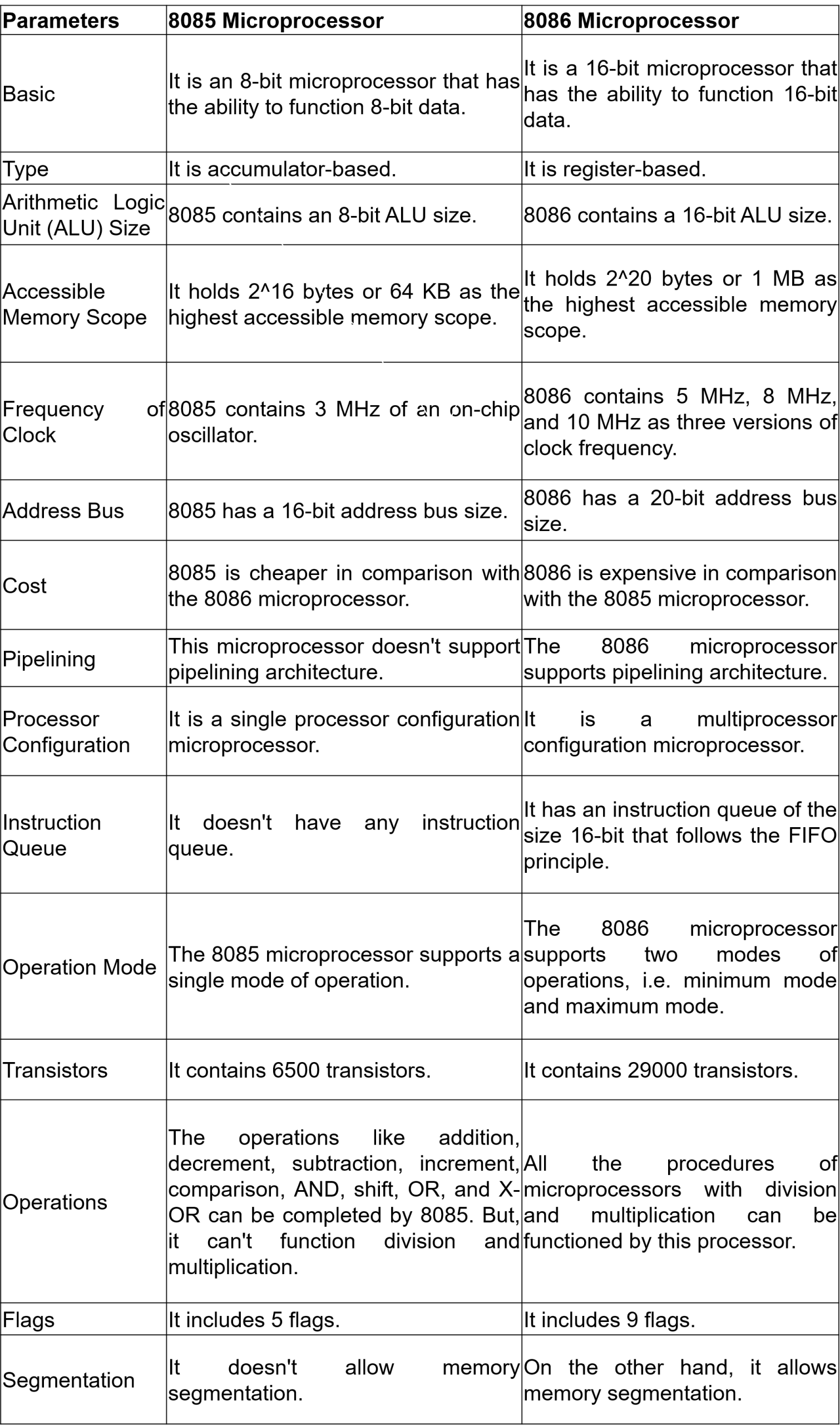
It was designed in 1976 by Intel. It is an 8-bit microprocessor with an 8-bit data bus, allowing it to handle 8 bits of data in a single cycle. A 16-bit address bus is present. As a result, it has a potential accessible memory capacity of 64 kilobytes, or 2^16 bytes.
In 1976, Intel came up with the idea. As a result of its 16-bit microprocessor and 16-bit data bus it can process 16-bit of data in a single cycle. There is a 20-bit address bus on it. The maximum amount of accessible memory that it can hold is 1 MB, or 2^20 bytes. The microprocessor 8086 is an improved model of the 8085.
Difference Between 8085 and 8086 Microprocessor
8085 Microprocessor
এটি 1976 সালে Intel দ্বারা design করা হয়েছিল। এটি একটি 8-bit microprocessor যার 8-bit data bus রয়েছে, যা একক cycle-এ 8 bits data handle করতে পারে। একটি 16-bit address bus উপস্থিত আছে। ফলস্বরূপ, এর potential accessible memory capacity 64 kilobytes বা 2^16 bytes।
8086 Microprocessor
1976 সালে Intel এটি তৈরির idea দেয়। এর 16-bit microprocessor এবং 16-bit data bus এর কারণে এটি একক cycle-এ 16-bit data process করতে পারে। এতে একটি 20-bit address bus রয়েছে। এটি সর্বোচ্চ 1 MB বা 2^20 bytes accessible memory ধারণ করতে পারে। Microprocessor 8086 হলো 8085-এর একটি উন্নত model।

Previous QnS on Microprocessor and Computer Architecture
- ☆1Microprocessor & Computer ArchitectureConsider a disk with a sector size of 512 bytes, 2000 tracks pér surface, 50 sectors per track, five double-sided platters, and average seek time of 10 msec. What is the capacity of a track in bytes? What is the capacity of each surface? What is the capacity of the disk?CB, SO(IT), 22 | Senior Officer (IT)
Capacity of a Track
Bytes per Track = Bytes per Sector × Sectors per Track
Bytes per Track = 512 × 50 = 25,600 bytesCapacity of a Surface
Bytes per Surface = Bytes per Track × Tracks per Surface
Bytes per Surface = 25,600 × 2000 = 51,200,000 bytes (50,000 KB)Capacity of the Disk
Bytes per Disk = Bytes per Surface × Number of Surfaces
Number of Surfaces = 5 Platters × 2 Surfaces per Platter = 10 Surfaces
Bytes per Disk = 51,200,000 × 10 = 512,000,000 bytes (500,000 KB)
- ☆2Microprocessor & Computer ArchitectureHits ratio 75%, RAM time 10 ns , SSD time 10 ms for each instruction. Calcualte access time.CB, AE(IT)/AHME/SO, 21 | AME/ANE/AE
Given:
- Hit Ratio = 75% = 0.75
- RAM Access Time = 10 ns = 10 × 10-9 seconds
- SSD Access Time = 10 ms = 10 × 10-3 seconds
We Know
Average Access Time = (Hit Ratio × RAM Time) + (Miss Ratio × SSD Time)
Miss Ratio = 1 - Hit Ratio = 1 - 0.75 = 0.25
Calculation:
Average Access Time = (0.75 × 10 × 10-9) + (0.25 × 10 × 10-3)
= 7.5 × 10⁻⁹ + 2.5 × 10-3
= 0.0000000075 + 0.0025 = 0.0025000075 seconds=0.0025000075 × 1000 = 2.5000075 ms
Average Access Time ≈ 2.5 milliseconds
Given:
- Hit Ratio = 75% = 0.75
- RAM Access Time = 10 ns = 10 × 10-9 seconds
- SSD Access Time = 10 ms = 10 × 10-3 seconds
We Know
Average Access Time = (Hit Ratio × RAM Time) + (Miss Ratio × SSD Time)
Miss Ratio = 1 - Hit Ratio = 1 - 0.75 = 0.25
Calculation:
Average Access Time = (0.75 × 10 × 10-9) + (0.25 × 10 × 10-3)
= 7.5 × 10⁻⁹ + 2.5 × 10-3
= 0.0000000075 + 0.0025 = 0.0025000075 seconds=0.0025000075 × 1000 = 2.5000075 ms
Average Access Time ≈ 2.5 milliseconds
- ☆3Microprocessor & Computer ArchitectureConsider a hard disk with: 4 surfaces, 64 tracks/surface, 128 sectors/track, 256 ytes/sector, what is the capacity of the hard disk?Janata, ASA, 21 | AME/ANE/AE
Given:
Surfaces = 4
Tracks per surface = 64
Sectors per track = 128
Bytes per sector = 256 bytesDisk Capacity Formula:
Capacity = Surfaces × Tracks per surface × Sectors per track × Bytes per sectorTotal sectors = 4 × 64 × 128
= 256 × 128
= 32,768 sectorsTotal capacity = 32,768 × 256 bytes
= 8,388,608 bytesConvert to MB:
1 MB = 1,048,576 bytes
8,388,608 ÷ 1,048,576 = 8 MB
Answer:
Disk Capacity ≈ 8 MB
- ☆4Microprocessor & Computer ArchitectureConsider disk pack with the following specification- 16 surfaces, 128 tracks per surfavce, 256 sectors per track and 512 bytes per sector. Answer the follwoing question.
(i) What is the capacity of disk pack?
(ii) If the format overhead is 32 bytes per sector, what is the formatted disk space?
(iii)If the disk is rotating at 3600 RPM, what is the data transfer rate?Rupali, ANE, 21 |Solution:
Data:
Number of surfaces = 16 = 24
Number of tracks per surface = 128 = 27
Number of sectors per track = 256 = 28
Number of bytes per sector = 512 = 29
Format overhead = 32 bytes per sector
Rotation speed = 3600 RPM(i) Capacity of the Disk Pack:
Capacity of the disk = Number of surfaces × Number of tracks × Number of sectors × Number of bytes per sector
= 24 × 27 × 28 × 29
= 228 bytes
= 268,435,456 bytes
= 256 MB
Therefore, the capacity of the disk pack = 256 MB.
Number of Sectors:
Number of sectors = Number of surfaces × Number of tracks × Number of sectors per track
= 24 × 27 × 28
= 219 sectors
Therefore, 19 bits are required to address all the sectors.
(ii) Formatted Disk Space:
Format overhead per sector = 32 bytes
Usable bytes per sector = 512 − 32 = 480 bytes
Formatted disk space = Total number of sectors × Usable bytes per sector
= 219 × 480
= 251,658,240 bytes
= 240 MB
Therefore, the formatted disk space = 251,658,240 bytes ≈ 240 MB.
(iii) Data Transfer Rate:
Rotation speed = 3600 RPM
Number of rotations in one second = 3600 ÷ 60 = 60 rotations/sec
Data transfer rate = Number of heads × Capacity of one track × Number of rotations in one second
= 16 × (256 × 512) × 60 bytes/sec
= 24 × 28 × 29 × 60 bytes/sec
= 60 × 221 bytes/sec
= 125,829,120 bytes/sec
= 120 MB/sec
Therefore, the Data Transfer Rate = 120 MB/sec.
- ☆5Microprocessor & Computer ArchitectureA system uses 16-bit logical address and a page size of 1 KB.
(i) How many pages are in the logical address space?
(ii) How many bits are used for the page number and offset?Dwasa,AME,25 | Other16-bit Logical Address and 1 KB Page SizeGiven:
- Logical Address Size = 16 bits
- Page Size = 1 KB = 210 bytes
(i) How many pages are in the logical address space?
First, calculate the total logical address space:
Total Address Space = 216 bytes
Since each page contains 210 bytes:
Number of Pages = 216 / 210
= 216 − 10
= 26 = 64 pages
Therefore, the logical address space contains 64 pages.
(ii) How many bits are used for the page number and offset?
The logical address is divided into two parts:
- Page Number: Identifies which page the address belongs to.
- Offset: Identifies the exact location within that page.
Since there are 64 pages:
Page Number Bits = log2(64) = 6 bits
Since the page size is 1 KB = 210 bytes:
Offset Bits = log2(210) = 10 bits
Therefore:
- Page Number = 6 bits
- Page Offset = 10 bits
- Total = 6 + 10 = 16 bits
Final Answer:
- Number of Pages = 64
- Page Number Bits = 6
- Offset Bits = 10
- ☆6Microprocessor & Computer ArchitectureWhy Heterogeneous Multicore Processor (HMP) gaining more popularity?CB, SO(IT), 20 | Senior Officer (IT)
A Heterogeneous Multicore Processor (HMP) contains different types of CPU cores, typically high-performance cores and power-efficient cores. It is becoming more popular because it provides a better balance between performance and energy efficiency.
1. Better Performance:
High-performance cores can handle demanding applications and computationally intensive tasks efficiently.2. Lower Power Consumption:
Power-efficient cores can handle lightweight tasks using less energy, which reduces overall power consumption.3. Improved Energy Efficiency:
The processor can assign each task to the most suitable type of core, providing high performance when needed while saving energy for less demanding tasks.4. Better Thermal Management:
Using efficient cores for lighter workloads reduces heat generation and helps maintain suitable operating temperatures.5. Suitable for Modern Devices:
HMP is especially useful in smartphones, laptops, servers, and embedded systems where both high performance and long battery life or lower operating cost are important.Conclusion:
HMP is gaining popularity because it provides high performance, lower power consumption, better energy efficiency, and improved thermal management by using different types of processor cores according to workload requirements.
Heterogeneous Multicore Processor (HMP)-এ বিভিন্ন ধরনের CPU Core থাকে। সাধারণত এতে High-Performance Core এবং Power-Efficient Core উভয়ই থাকে। এটি Performance এবং Energy Efficiency-এর মধ্যে ভালো ভারসাম্য তৈরি করে।
১. উন্নত Performance:
High-Performance Core ব্যবহার করে Computationally Intensive এবং কঠিন কাজ দ্রুত সম্পন্ন করা যায়।২. কম Power Consumption:
সাধারণ বা হালকা কাজগুলো Power-Efficient Core দিয়ে সম্পন্ন করা যায়, ফলে কম Energy ব্যবহার হয়।৩. উন্নত Energy Efficiency:
Processor প্রতিটি কাজের জন্য উপযুক্ত Core নির্বাচন করতে পারে। ফলে প্রয়োজনের সময় High Performance এবং সাধারণ কাজের সময় Energy Saving করা সম্ভব হয়।৪. উন্নত Thermal Management:
হালকা কাজ Efficient Core-এ সম্পন্ন করলে কম Heat উৎপন্ন হয় এবং Processor-এর Temperature নিয়ন্ত্রণে রাখা সহজ হয়।৫. আধুনিক Device-এর জন্য উপযোগী:
Smartphone, Laptop, Server এবং Embedded System-এ HMP বিশেষভাবে কার্যকর, কারণ এসব ক্ষেত্রে High Performance-এর পাশাপাশি কম Power Consumption গুরুত্বপূর্ণ।উপসংহার:
HMP জনপ্রিয় হচ্ছে কারণ এটি বিভিন্ন ধরনের Core ব্যবহার করে উচ্চ Performance, কম Power Consumption, উন্নত Energy Efficiency এবং ভালো Thermal Management প্রদান করে।
- ☆7Microprocessor & Computer ArchitectureWhat is block and page? Draw simple block and page diagram in SSD (Solid State Drive).CB, SO(IT), 20 | Senior Officer (IT)
In a Solid State Drive (SSD), data is stored in flash memory. The flash memory is organized into Pages and Blocks.
1. Page:
A Page is the smallest unit of data that can normally be read or programmed (written) in NAND flash memory. A page typically contains several KB of data.2. Block:
A Block is a group of multiple pages. The erase operation in NAND flash memory is normally performed at the block level.SSD (NAND Flash Memory) | +----------------+----------------+ | | BLOCK 1 BLOCK 2 | | +----+----+ +----+----+ | | | | | | Page 1 Page 2 Page 3 ... Page 1 Page 2 Page 3 ... | | | | | | 4 KB 4 KB 4 KB 4 KB 4 KB 4 KBPage: A Page is the basic unit for reading and writing data in NAND flash memory.
Block: A Block is a group of multiple Pages and is the basic unit for erase operations.
- ☆8Microprocessor & Computer ArchitectureWrite are the parameters that are being used to evaluate the performance of memory?CB, SO(IT), 20 | Senior Officer (IT)
Parameters Used to Evaluate Memory Performance
The performance of a computer memory is evaluated using several important parameters:
1. Access Time:
It is the time required to locate and access a particular data item from memory. Lower access time means faster memory.2. Memory Cycle Time:
It is the minimum time interval required between two successive memory operations.3. Transfer Rate:
It indicates the amount of data that can be transferred between memory and the processor per unit of time. Higher transfer rate means better performance.4. Memory Capacity:
It represents the total amount of data that the memory can store, usually measured in KB, MB, GB, or TB.5. Cost per Bit:
It represents the cost of storing one bit of information. A lower cost per bit generally makes a memory technology more economical.6. Bandwidth:
It represents the amount of data that can be transferred by the memory in a given period, usually expressed in bytes per second.Conclusion:
The major parameters used to evaluate memory performance are Access Time, Memory Cycle Time, Transfer Rate, Capacity, Cost per Bit, and Bandwidth.
Memory-এর Performance মূল্যায়নের Parameters
Computer Memory-এর Performance মূল্যায়নের জন্য কয়েকটি গুরুত্বপূর্ণ Parameter ব্যবহার করা হয়:
১. Access Time:
Memory থেকে নির্দিষ্ট Data খুঁজে বের করে Access করতে যে সময় লাগে তাকে Access Time বলে। Access Time কম হলে Memory দ্রুত কাজ করে।২. Memory Cycle Time:
পরপর দুটি Memory Operation-এর মধ্যে প্রয়োজনীয় সর্বনিম্ন সময়কে Memory Cycle Time বলে।৩. Transfer Rate:
প্রতি একক সময়ে Memory এবং Processor-এর মধ্যে কত পরিমাণ Data Transfer করা যায় তাকে Transfer Rate বলে। Transfer Rate বেশি হলে Performance ভালো হয়।৪. Memory Capacity:
Memory সর্বমোট কত পরিমাণ Data সংরক্ষণ করতে পারে তাকে Memory Capacity বলে। এটি সাধারণত KB, MB, GB বা TB-তে প্রকাশ করা হয়।৫. Cost per Bit:
এক Bit Data সংরক্ষণ করতে যে খরচ হয় তাকে Cost per Bit বলে। Cost per Bit কম হলে Memory তুলনামূলকভাবে বেশি সাশ্রয়ী।৬. Bandwidth:
নির্দিষ্ট সময়ে Memory কত পরিমাণ Data Transfer করতে পারে তাকে Memory Bandwidth বলে। এটি সাধারণত Bytes per Second-এ প্রকাশ করা হয়।উপসংহার:
Memory Performance মূল্যায়নের প্রধান Parameter হলো Access Time, Memory Cycle Time, Transfer Rate, Capacity, Cost per Bit এবং Bandwidth।
- ☆9Microprocessor & Computer ArchitectureBasicA server has a fast CPU and abundant RAM, but despite low CPU and memory utilization, the system suffers from severe instruction execution delays and high latency during processing tasks. What needs to be updated, and what is the solution?ICB, AP, 26 | Assistant Programmer
When CPU and RAM utilization are low but system latency is high, the bottleneck is not compute or memory, but input/output performance.
Step 1: Identify bottleneck
- Low CPU usage → not compute-bound
- Low memory usage → not memory-bound
- High latency → likely I/O-bound system
Step 2: Root cause
Slow disk storage (HDD), high I/O wait time, and limited throughput are common causes.
Solution:
Upgrade storage subsystem to SSD or NVMe and optimize I/O scheduling.
Conclusion: I/O subsystem is the critical bottleneck, not CPU or RAM.
Performance Bottleneck Analysis
CPU ও RAM কম ব্যবহার হলেও latency বেশি হলে এটি I/O bottleneck নির্দেশ করে।
সমস্যা:
- Slow HDD storage
- High I/O wait
Solution: SSD/NVMe storage upgrade ও I/O optimization।
- ☆10Microprocessor & Computer ArchitectureBasicWhat exactly is a microcontroller? What distinguishes a microprocessor from a microcontroller? Mention the differences between RISC and CISC microprocessors.Combined Bank, SO(IT), 24 | Senior Officer (IT)
A microcontroller is a small, low-cost microcomputer designed to perform specific tasks in embedded systems. It integrates a processor, memory (RAM, ROM, EPROM), and peripherals such as timers, counters, and serial ports into a single chip. Microcontrollers are commonly used in applications like microwave ovens, remote controls, and IoT devices.
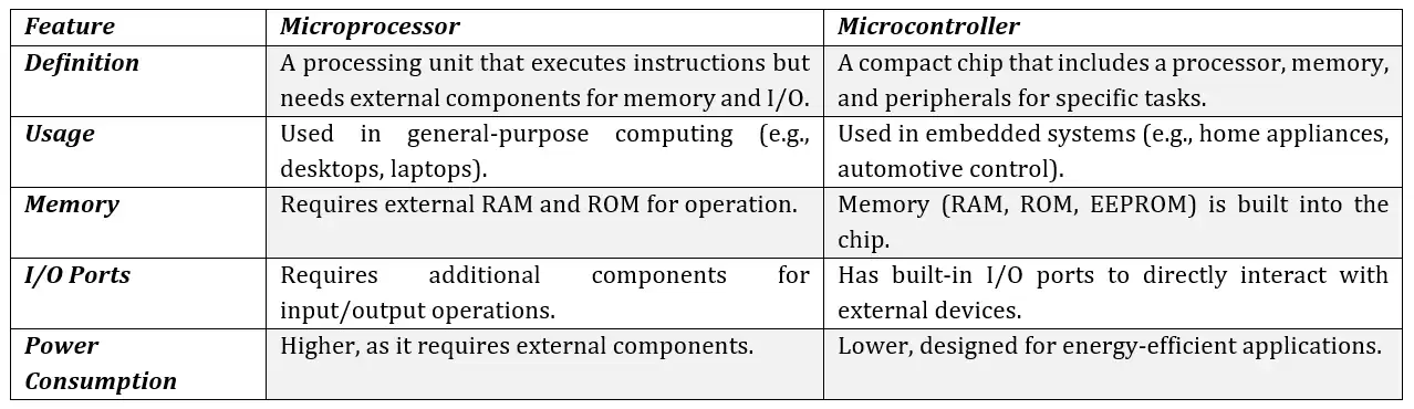
Difference Between Microprocessor and Microcontroller
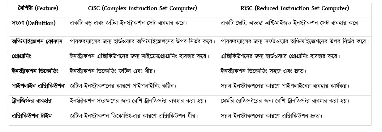
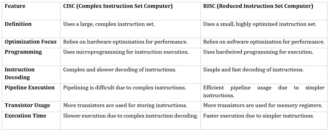
Differences Between RISC and CISC Microprocessors
📖 For More Details about this topic
- ☆11Microprocessor & Computer ArchitectureBasicDifference between 32 bit Microprocessor and 64 bit Microprocessor with example. What is the meaning of 2.40GHz Microprocessor? Differentiate among Core Indel i3, i5 and i7 processor. Why do you prefer SSD instead of HDD? 10CB, SO(IT), 23 | Senior Officer (IT)
Difference between 32-bit and 64-bit Microprocessor
32-bit Microprocessor
- Supports maximum 4 GB RAM.
- Uses 32-bit address space.
- Limited support for modern software.
- Lower performance compared to 64-bit.
- Less expensive.
- Examples: Motorola 68020, HP FOCUS.
64-bit Microprocessor
- Supports very large RAM (terabytes).
- Uses 64-bit address space.
- Better performance and multitasking.
- Supports modern 64-bit software.
- More expensive.
- Examples: AMD Opteron, Intel x64 series.
Meaning of 2.40 GHz Microprocessor
2.40 GHz means the processor can execute 2.40 billion clock cycles per second, indicating higher processing speed.
Difference among Intel Core i3, i5, and i7
Intel Core i3
- Entry-level processor.
- Usually 2–4 cores.
- No Turbo Boost.
- Best for basic tasks.
Intel Core i5
- Mid-range processor.
- 4–6 cores.
- Supports Turbo Boost.
- Good for multitasking.
Intel Core i7
- High-performance processor.
- 6–8+ cores.
- Supports Hyper-Threading and Turbo Boost.
- Best for heavy applications.
Why prefer SSD instead of HDD?
SSD provides faster speed, better durability, low power consumption, and silent operation. HDD is cheaper but slower and less reliable.
32-bit ও 64-bit Microprocessor-এর পার্থক্য
32-bit Microprocessor
- সর্বোচ্চ 4 GB RAM সাপোর্ট করে।
- 32-bit address space ব্যবহার করে।
- নতুন software-এর সাপোর্ট সীমিত।
- পারফরম্যান্স তুলনামূলক কম।
- দাম কম।
- উদাহরণ: Motorola 68020, HP FOCUS।
64-bit Microprocessor
- অনেক বেশি RAM (TB পর্যন্ত) সাপোর্ট করে।
- 64-bit address space ব্যবহার করে।
- উচ্চ পারফরম্যান্স ও multitasking সুবিধা।
- আধুনিক software সাপোর্ট করে।
- দাম বেশি।
- উদাহরণ: AMD Opteron, Intel x64।
2.40 GHz Microprocessor-এর অর্থ
2.40 GHz মানে processor প্রতি সেকেন্ডে 2.40 বিলিয়ন clock cycle সম্পন্ন করতে পারে।
Intel Core i3, i5 ও i7-এর পার্থক্য
Intel Core i3
- Entry-level processor।
- কম core সংখ্যা।
- Turbo Boost নেই।
- Basic কাজের জন্য উপযোগী।
Intel Core i5
- Mid-range processor।
- Turbo Boost সাপোর্ট করে।
- Multitasking-এর জন্য ভালো।
Intel Core i7
- High-performance processor।
- বেশি core ও thread।
- Heavy application-এর জন্য উপযোগী।
HDD-এর পরিবর্তে SSD কেন ব্যবহার করা হয়?
SSD দ্রুত কাজ করে, টেকসই, কম বিদ্যুৎ ব্যবহার করে এবং শব্দহীন। তাই আধুনিক কম্পিউটারে SSD বেশি ব্যবহৃত হয়।
- ☆12Microprocessor & Computer ArchitectureBasicDifferentiate among CPU register, Cache memory, Main memory and Secondary memory. 10CB, SO(IT), 23 | Senior Officer (IT)
CPU Register: Registers are small and extremely fast storage locations inside the CPU. They temporarily hold data and instructions that are currently being processed, enabling faster execution. Examples include Data Register, Address Register, and Accumulator.
Cache Memory: Cache memory is a high-speed memory located close to the CPU. It stores frequently used data and instructions to reduce access time and improve system performance. Cache memory is faster than RAM but smaller in size.
Main Memory: Main memory, commonly known as RAM, stores data and programs that are actively in use. It is larger than cache memory but slower. Main memory is volatile, meaning data is lost when power is turned off. Examples include RAM, ROM, PROM, and EPROM.
Secondary Memory: Secondary memory is used for permanent data storage. It is slower than main memory and not directly accessed by the CPU. Data must first be loaded into main memory before processing. Examples include Hard Disk, SSD, Flash Drive, and Optical Disk.
CPU Register: Register হলো CPU-এর ভেতরে থাকা ছোট ও অত্যন্ত দ্রুতগতির memory। এটি বর্তমানে process হওয়া data ও instruction সাময়িকভাবে সংরক্ষণ করে, ফলে CPU দ্রুত কাজ করতে পারে। উদাহরণ: Data Register, Address Register এবং Accumulator।
Cache Memory: Cache memory হলো খুব দ্রুতগতির memory যা CPU-এর কাছাকাছি থাকে। এতে বারবার ব্যবহৃত data ও instruction সংরক্ষণ করা হয়, ফলে CPU দ্রুত access করতে পারে এবং system performance বৃদ্ধি পায়。
Main Memory: Main memory বা RAM হলো কম্পিউটারের প্রধান memory যেখানে চলমান program ও data সংরক্ষিত থাকে। এটি cache memory থেকে বড় কিন্তু তুলনামূলক ধীর। এটি volatile, অর্থাৎ বিদ্যুৎ বন্ধ হলে data নষ্ট হয়ে যায়। উদাহরণ: RAM, ROM, PROM এবং EPROM।
Secondary Memory: Secondary memory স্থায়ীভাবে data সংরক্ষণের জন্য ব্যবহৃত হয়। এটি main memory থেকে ধীর এবং CPU সরাসরি access করতে পারে না। আগে data main memory-তে আনতে হয়। উদাহরণ: Hard Disk, SSD, Flash Drive এবং Optical Disk।
- ☆13Microprocessor & Computer ArchitectureBasicCompare RAM, ROM, cache memory, and secondary storage in terms of speed and usage.Combined Bank, O(IT-23), 26 | Officer (IT)
RAM (Random Access Memory)
- RAM is the primary memory of a computer used to temporarily store data and programs currently being processed by the CPU.
- It is volatile memory, meaning its data is lost when the power is turned off.
- RAM provides fast read and write operations, allowing applications and the operating system to run efficiently.
Usage: Running applications, operating systems, and temporary data processing.
ROM (Read Only Memory)
- ROM is non-volatile memory that permanently stores instructions required for booting and hardware initialization.
- The data stored in ROM remains even after power is turned off.
- ROM usually contains firmware or BIOS programs.
Usage: System startup and firmware storage.
Cache Memory
- Cache memory is a very small but extremely fast memory located inside or close to the CPU.
- It stores frequently used instructions and data so the CPU can access them quickly without waiting for RAM.
- Cache memory improves processor speed and overall system performance.
Usage: Temporary storage of frequently accessed CPU data and instructions.
Secondary Storage
- Secondary storage is non-volatile storage used for permanent data storage.
- It stores files, operating systems, software, videos, documents, and backups for long-term use.
Examples include HDD, SSD, DVD, memory cards, and pen drives.
Usage: Permanent storage of data and applications.
Cache Memory → RAM → ROM → Secondary Storage

RAM (Random Access Memory)
- RAM হলো computer-এর primary memory যেখানে CPU বর্তমানে ব্যবহৃত data এবং program সাময়িকভাবে সংরক্ষণ করে।
- এটি volatile memory, অর্থাৎ power বন্ধ হলে data মুছে যায়।
- RAM দ্রুত read এবং write operation প্রদান করে, ফলে application এবং operating system দ্রুত কাজ করতে পারে।
ব্যবহার: Application চালানো, operating system এবং temporary data processing।
ROM (Read Only Memory)
- ROM হলো non-volatile memory যেখানে system booting এবং hardware initialization-এর জন্য প্রয়োজনীয় instruction স্থায়ীভাবে সংরক্ষণ করা হয়।
- Power বন্ধ হলেও ROM-এর data মুছে যায় না।
- ROM সাধারণত firmware বা BIOS program ধারণ করে।
ব্যবহার: System startup এবং firmware storage।
Cache Memory
- Cache memory হলো খুব ছোট কিন্তু অত্যন্ত দ্রুত memory যা CPU-এর ভিতরে বা কাছাকাছি থাকে।
- এটি frequently used instruction এবং data সংরক্ষণ করে যাতে CPU দ্রুত access করতে পারে এবং RAM-এর জন্য অপেক্ষা করতে না হয়।
- Cache memory processor speed এবং overall performance বৃদ্ধি করে।
ব্যবহার: Frequently accessed CPU data এবং instruction-এর temporary storage।
Secondary Storage
- Secondary storage হলো non-volatile storage যা permanent data storage-এর জন্য ব্যবহৃত হয়।
- এতে file, operating system, software, video, document এবং backup দীর্ঘমেয়াদে সংরক্ষণ করা হয়।
- উদাহরণ: HDD, SSD, DVD, memory card এবং pen drive।
ব্যবহার: Data এবং application স্থায়ীভাবে সংরক্ষণ।
Memory Speed Hierarchy
Cache Memory → RAM → ROM → Secondary Storage

- ☆14Microprocessor & Computer ArchitectureBasicDiscuss the factors that affect the Speed of a CPU.Rupali, ANE, 23 | AME/ANE/AE
Factors Affecting the Speed of a CPU
The speed of a CPU determines how fast a computer can process instructions. Several hardware and architectural factors influence CPU speed.
1. Clock Speed
Clock speed, measured in GHz, indicates how many cycles a CPU can perform per second. Higher clock speed generally means faster processing.
2. Number of Cores
Modern CPUs have multiple cores, allowing them to execute multiple tasks simultaneously. More cores improve multitasking and performance.
3. Cache Memory
Cache memory stores frequently used data close to the CPU. Larger cache size reduces access time and increases processing speed.
4. Word Length
Word length refers to the number of bits a CPU can process at a time. A 64-bit CPU can handle more data than a 32-bit CPU.
5. Bus Speed
Bus speed determines how fast data is transferred between the CPU, memory, and other components. Higher bus speed improves overall performance.
6. CPU Architecture
Efficient architecture, such as pipelining and instruction-level parallelism, allows the CPU to execute instructions faster.
CPU-এর Speed প্রভাবিতকারী বিষয়সমূহ
CPU-এর speed নির্ধারণ করে একটি computer কত দ্রুত instruction process করতে পারবে। CPU-এর speed বিভিন্ন hardware ও architectural বিষয়ের উপর নির্ভর করে।
১. Clock Speed
Clock speed GHz এককে পরিমাপ করা হয় এবং এটি CPU প্রতি সেকেন্ডে কতটি cycle সম্পন্ন করতে পারে তা নির্দেশ করে। Clock speed যত বেশি, CPU তত দ্রুত কাজ করে।
২. Number of Cores
একটি CPU-তে একাধিক core থাকলে একই সময়ে একাধিক কাজ করা যায়। Core সংখ্যা বেশি হলে multitasking performance ভালো হয়।
৩. Cache Memory
Cache memory CPU-এর খুব কাছে থাকে এবং frequently used data সংরক্ষণ করে। Cache বেশি হলে data access দ্রুত হয়।
৪. Word Length
Word length হলো CPU একবারে কত bit data process করতে পারে। 64-bit CPU, 32-bit CPU-এর চেয়ে বেশি data handle করতে পারে।
৫. Bus Speed
Bus speed CPU এবং memory-এর মধ্যে data transfer-এর গতি নির্ধারণ করে। Bus speed বেশি হলে system performance বাড়ে।
৬. CPU Architecture
Advanced architecture যেমন pipelining ও parallel processing CPU-কে দ্রুত instruction execute করতে সাহায্য করে।
- ☆15Microprocessor & Computer ArchitecturePipeliningWhy do modern processor designs favor a multi-stage pipelined approach over a single-cycle implementation?Combined Bank, SO(IT-24), 26 | Senior Officer (IT)
Modern processors favor a Multi-Stage Pipelined Architecture because it improves performance by allowing multiple instructions to be executed simultaneously. Instead of completing one instruction in a single long clock cycle, the processor divides instruction execution into several stages, such as Instruction Fetch (IF), Instruction Decode (ID), Execute (EX), Memory Access (MEM), and Write Back (WB).
Reasons for Using Multi-Stage Pipelining
• Higher Throughput: Multiple instructions are processed simultaneously in different pipeline stages.
• Shorter Clock Cycle: Each stage performs a smaller task, allowing a higher clock frequency.
• Better CPU Utilization: Different hardware units remain active instead of waiting for one instruction to complete.
• Higher Performance: After the pipeline is filled, ideally one instruction completes in every clock cycle.
• Improved Scalability: Supports deeper pipelines and advanced processor optimizations in modern CPUs.Comparison
Single-Cycle Processor Multi-Stage Pipelined Processor Executes one instruction in one long clock cycle. Executes multiple instructions simultaneously in different pipeline stages. Long clock cycle. Short clock cycle. Lower throughput. Higher throughput. Lower hardware utilization. Higher hardware utilization. Lower overall performance. Higher overall performance. Modern processors use Multi-Stage Pipelining because it increases throughput, improves CPU utilization, supports higher clock speeds, and provides significantly better performance than a Single-Cycle implementation.
আধুনিক Processor-এ Multi-Stage Pipelining ব্যবহার করা হয়, কারণ এটি একই সময়ে একাধিক Instruction বিভিন্ন Stage-এ Execute করতে পারে, ফলে System-এর Performance উল্লেখযোগ্যভাবে বৃদ্ধি পায়। এখানে একটি Instruction-কে Instruction Fetch (IF), Instruction Decode (ID), Execute (EX), Memory Access (MEM) এবং Write Back (WB) Stage-এ ভাগ করে Process করা হয়।
Multi-Stage Pipelining ব্যবহারের কারণ
• উচ্চ Throughput: একই সময়ে বিভিন্ন Stage-এ একাধিক Instruction Process করা যায়।
• ছোট Clock Cycle: প্রতিটি Stage অল্প কাজ সম্পন্ন করে, ফলে উচ্চ Clock Frequency ব্যবহার করা সম্ভব হয়।
• উন্নত CPU Utilization: Processor-এর বিভিন্ন Hardware Unit একসাথে কাজ করতে পারে।
• উচ্চ Performance: Pipeline পূর্ণ হওয়ার পরে প্রায় প্রতি Clock Cycle-এ একটি Instruction সম্পন্ন হয়।
• ভালো Scalability: আধুনিক CPU-তে Deep Pipeline এবং Advanced Optimization Technique ব্যবহার করা যায়।তুলনা
Single-Cycle Processor Multi-Stage Pipelined Processor একটি দীর্ঘ Clock Cycle-এ একটি Instruction Execute করে। বিভিন্ন Pipeline Stage-এ একই সাথে একাধিক Instruction Execute করে। Clock Cycle দীর্ঘ। Clock Cycle ছোট। Throughput কম। Throughput বেশি। Hardware Utilization কম। Hardware Utilization বেশি। Overall Performance কম। Overall Performance বেশি। আধুনিক Processor-এ Multi-Stage Pipelining ব্যবহার করা হয়, কারণ এটি Throughput বৃদ্ধি করে, CPU Utilization উন্নত করে, উচ্চ Clock Speed সমর্থন করে এবং Single-Cycle Processor-এর তুলনায় অনেক বেশি দক্ষতা ও Performance প্রদান করে।
- ☆16Microprocessor & Computer ArchitecturePipeliningWhy do modern processor designs favor multistage pipeline approach over single cycle implementation? Explain with appropriate reasoning.Combined Bank, AE(IT)/AME, 26 | AME/ANE/AE
Single Cycle Processor :
- All steps of an instruction (fetch, decode, execute, memory, write back) are completed in one clock cycle.
- Clock cycle must be long enough to complete the slowest instruction.
Multistage Pipeline Processor :
- Instruction execution is divided into multiple stages (fetch, decode, execute, etc.).
- Multiple instructions are processed simultaneously in different stages.
Why Modern Processors Prefer Multistage Pipeline:
- Higher Throughput: Multiple instructions execute in parallel → more work done in less time.
- Faster Clock Speed: Each stage does small work → shorter clock cycle.
- Efficient Hardware Usage: Different units work at the same time → better utilization.
- Less Idle Time: Hardware is continuously active unlike single cycle.
- Supports Parallelism: Enables instruction-level parallelism (ILP).
- Better Performance: Overall execution is faster than single cycle design.
Single Cycle Processor :
- একটি instruction-এর সব ধাপ (fetch, decode, execute, memory, write back) একটি clock cycle-এ সম্পন্ন হয়।
- Clock cycle এমনভাবে সেট করতে হয় যাতে সবচেয়ে ধীর instruction সম্পন্ন হয়।
Multistage Pipeline Processor :
- Instruction execution-কে একাধিক stage-এ ভাগ করা হয় (fetch, decode, execute ইত্যাদি)।
- একই সময়ে ভিন্ন stage-এ একাধিক instruction process হয়।
Modern Processor কেন Multistage Pipeline ব্যবহার করে:
- উচ্চ Throughput: একসাথে একাধিক instruction execute হয় → সময় কম লাগে।
- দ্রুত Clock Speed: প্রতিটি stage ছোট কাজ করে → clock cycle ছোট হয়।
- Hardware এর ভালো ব্যবহার: সব unit একসাথে কাজ করে → efficiency বাড়ে।
- Idle Time কম: Single cycle-এর মতো hardware idle থাকে না।
- Parallelism: instruction-level parallelism (ILP) সম্ভব হয়।
- উচ্চ Performance: overall execution দ্রুত হয়।
- ☆17Microprocessor & Computer ArchitectureCache MemoryExplain the difference between a "Compulsory Miss" (Cold Miss) and a "Capacity Miss" in cache memory.Combined Bank, SO(IT-24), 26 | Senior Officer (IT)
A Cache Miss occurs when the required data is not found in the Cache Memory, forcing the processor to fetch the data from the slower Main Memory. Two common types of cache misses are Compulsory Miss (Cold Miss) and Capacity Miss.
Difference between Compulsory Miss and Capacity Miss
Compulsory Miss (Cold Miss) Capacity Miss Occurs when data is accessed for the first time. Occurs when the cache is too small to hold all the required data. Happens even if the cache is empty. Happens because previously stored data is replaced due to limited cache size. Cannot be avoided during the first access. Can be reduced by increasing the cache size. Also called Cold Start Miss. Also called Cache Capacity Miss. Example
Compulsory Miss: When a program accesses an array element for the first time, the data is not yet in the cache, resulting in a Compulsory Miss.
Capacity Miss: If a program processes a very large array that cannot fit entirely in the cache, old data is continuously replaced by new data, causing Capacity Misses.
যখন প্রয়োজনীয় Data Cache Memory-তে পাওয়া যায় না এবং Processor-কে Main Memory থেকে Data আনতে হয়, তখন তাকে Cache Miss বলা হয়। Compulsory Miss (Cold Miss) এবং Capacity Miss হলো Cache Miss-এর দুটি গুরুত্বপূর্ণ ধরন।
Compulsory Miss এবং Capacity Miss-এর পার্থক্য
Compulsory Miss (Cold Miss) Capacity Miss কোনো Data প্রথমবার Access করলে ঘটে। Cache-এর Capacity পর্যাপ্ত না হলে ঘটে। Cache খালি থাকলেও প্রথম Access-এ এই Miss ঘটে। Cache পূর্ণ হয়ে গেলে পুরোনো Data Replace হওয়ার কারণে এই Miss ঘটে। প্রথম Access-এর সময় এটি এড়ানো যায় না। Cache-এর Size বৃদ্ধি করলে এটি কমানো যায়। এটিকে Cold Start Missও বলা হয়। এটিকে Cache Capacity Missও বলা হয়। উদাহরণ
Compulsory Miss: একটি Program যখন প্রথমবার কোনো Array-এর Element Access করে, তখন সেই Data Cache-এ না থাকায় Compulsory Miss ঘটে।
Capacity Miss: যদি একটি বড় Array-এর Size Cache-এর Capacity-এর চেয়ে বেশি হয়, তাহলে নতুন Data আনার জন্য পুরোনো Data বারবার Replace হয়, ফলে Capacity Miss ঘটে।
- ☆18Microprocessor & Computer ArchitectureMemory ManagementA system has a very fast CPU but slow main memory, explain how memory hierarchy helps reduce the performance gap between CPU and memory.Combined Bank, AE(IT)/AME, 26 | AME/ANE/AE
Memory Hierarchy :
- Memory hierarchy is an arrangement of different types of memory (Cache, RAM, Secondary Storage) based on speed, cost, and size.
- Faster memory is placed closer to CPU and slower memory is placed farther away.
How It Reduces CPU–Memory Gap:
- Use of Cache Memory: Frequently used data is stored in Cache (very fast) → CPU accesses data quickly.
- Temporal Locality: Recently used data is likely to be used again → kept in cache.
- Spatial Locality: Nearby data is also loaded → reduces repeated memory access.
- Reduced Access Time: CPU mostly accesses cache instead of slow main memory.
- Layered Access: If data not in cache → check RAM → then secondary storage.
- Improved Performance: Overall system speed increases by minimizing slow memory access.
Memory Hierarchy :
- Memory hierarchy হলো বিভিন্ন ধরনের memory (Cache, RAM, Secondary Storage)-এর একটি বিন্যাস, যা speed, cost এবং size অনুযায়ী সাজানো হয়।
- দ্রুত memory CPU-এর কাছে থাকে এবং ধীর memory দূরে থাকে।
কিভাবে CPU–Memory gap কমায়:
- Cache Memory ব্যবহার: বেশি ব্যবহৃত data Cache-এ রাখা হয় → CPU দ্রুত access করতে পারে।
- Temporal Locality: সম্প্রতি ব্যবহৃত data আবার ব্যবহার হওয়ার সম্ভাবনা বেশি → cache-এ রাখা হয়।
- Spatial Locality: কাছাকাছি data একসাথে load হয় → বারবার memory access কমে।
- Access Time কমে: CPU বেশি সময় cache ব্যবহার করে → slow RAM কম ব্যবহার হয়।
- Layer অনুযায়ী access: Cache → RAM → Secondary Storage এইভাবে খোঁজা হয়।
- Performance বৃদ্ধি: slow memory access কমিয়ে overall system দ্রুত হয়।
- ☆19Microprocessor & Computer ArchitectureOthersDifference between Multi Computer System and Multi Processor System. What is Pipelining? Explain the four stages of a Pipeline. Describe PPI.CB, AE(IT)/AME, 24 | AME/ANE/AE
Difference Between Multiprocessor System and Multicomputer System
- Definition: Multiprocessor = multiple CPUs sharing a single memory; Multicomputer = multiple independent computers connected via network.
- Memory: Multiprocessor uses shared memory; Multicomputer uses distributed memory.
- Communication: Multiprocessor uses shared memory; Multicomputer uses message passing.
- Coupling: Multiprocessor is tightly coupled; Multicomputer is loosely coupled.
- Example: Multiprocessor → Multi-core CPU system; Multicomputer → Cluster system.
Pipelining (Definition)
- Pipelining is a technique where multiple instructions are processed simultaneously in different stages of execution.
- It increases throughput by overlapping instruction execution.
4 Stages of Pipeline
- 1. Instruction Fetch (IF): Fetch instruction from memory.
- 2. Instruction Decode (ID): Decode instruction and identify operands.
- 3. Execute (EX): Perform operation (ALU processing).
- 4. Write Back (WB): Store result back to register/memory.
PPI (Parallel Processing Interface)
- PPI is a system where multiple processors or units work simultaneously to perform tasks.
- It improves performance and speed by dividing tasks into smaller parts.
- Used in applications like scientific computing, data processing.
Multiprocessor System এবং Multicomputer System-এর পার্থক্য
- সংজ্ঞা: Multiprocessor = একাধিক CPU একটি memory share করে; Multicomputer = একাধিক independent computer network দিয়ে যুক্ত।
- Memory: Multiprocessor-এ shared memory; Multicomputer-এ distributed memory।
- Communication: Multiprocessor-এ shared memory; Multicomputer-এ message passing।
- Coupling: Multiprocessor tightly coupled; Multicomputer loosely coupled।
- উদাহরণ: Multiprocessor → multi-core system; Multicomputer → cluster system।
Pipelining (সংজ্ঞা)
- Pipelining হলো এমন একটি technique যেখানে একাধিক instruction একই সময়ে ভিন্ন stage-এ process হয়।
- এটি throughput বাড়ায় কারণ instruction overlap হয়।
Pipeline-এর ৪টি Stage
- 1. Instruction Fetch (IF): memory থেকে instruction আনা হয়।
- 2. Instruction Decode (ID): instruction decode করে operand নির্ধারণ করা হয়।
- 3. Execute (EX): operation সম্পন্ন করা হয় (ALU কাজ করে)।
- 4. Write Back (WB): result register বা memory-এ সংরক্ষণ করা হয়।
PPI (Parallel Processing Interface)
- PPI হলো এমন একটি system যেখানে একাধিক processor একসাথে parallelভাবে কাজ করে।
- এটি কাজকে ভাগ করে performance ও speed বাড়ায়।
- ব্যবহার: scientific computing, data processing ইত্যাদি।
- ☆20Microprocessor & Computer ArchitectureOthersDefine Amdahl's law. How does it mathematically dictate the absolute maximum performance speedup a system can achieve when adding more cpu cores.RAKUB, ANSE, 26 | AME/ANE/AE
Amdahl's Law
Amdahl's Law is a formula that determines the theoretical maximum speedup of a system when only part of the system is improved. It highlights that overall performance is limited by the portion of a program that cannot be parallelized, regardless of how many processors are added.
Mathematical Formula
Speedup = 1 / [(1 − P) + (P / N)]
Where:
- P: Fraction of the program that can be parallelized (0 to 1)
- (1 − P): Sequential portion that cannot be parallelized
- N: Number of CPU cores (processors)
How It Limits Maximum Speedup
Amdahl's Law shows that even if we use infinite cores, the maximum speedup is limited by 1 / (1 − P). The sequential part of the program becomes the performance bottleneck.
- If P = 0.9: Maximum speedup = 1 / 0.1 = 10×
- If P = 0.5: Maximum speedup = 1 / 0.5 = 2×
- If P = 0.99: Maximum speedup = 1 / 0.01 = 100×
Example Calculation
Given: P = 0.7, N = 8
Speedup = 1 / [(1 − 0.7) + (0.7 / 8)]
Speedup = 1 / [0.3 + 0.0875]
Speedup = 1 / 0.3875 = 2.58×Even with 8 cores, performance gain is limited because the 30% sequential portion cannot be parallelized.
Key Insight:
Adding more cores leads to diminishing returns. To achieve higher speedup, the sequential portion of the program must be minimized.Amdahl's Law
Amdahl's Law হলো একটি formula যা system-এর theoretical maximum speedup calculate করে যখন শুধু এর একটি অংশ improve করা হয়। এটি দেখায় যে overall speedup program-এর যে অংশ parallelize করা যায় না সেই fraction দ্বারা limited, CPU cores যতই add করা হোক না কেন।
Mathematical Formula
Speedup = 1 / [(1 − P) + (P / N)]
Where:
- P: Program-এর যে fraction parallelize করা যায় (0 থেকে 1)
- (1 − P): যে fraction sequentially run করতে হবে এবং speed up করা যায় না
- N: CPU cores (processors)-এর সংখ্যা
Maximum Speedup কীভাবে Dictate করে
এই law একটি harsh truth reveal করে: infinite cores থাকলেও speedup কখনো 1 / (1 − P)-এর বেশি হতে পারে না। Sequential portion একটি hard ceiling হয়ে যায়।
- যদি P = 0.9: (90% parallelizable) → Maximum speedup = 1 / 0.1 = 10×
- যদি P = 0.5: (50% parallelizable) → Maximum speedup = 1 / 0.5 = 2×
- যদি P = 0.99: (99% parallelizable) → Maximum speedup = 1 / 0.01 = 100×
Example Calculation
A program spends 70% time in parallel tasks and 30% in sequential tasks. With 8 cores:
P = 0.7, N = 8
Speedup = 1 / [(1 − 0.7) + (0.7 / 8)]
Speedup = 1 / [0.3 + 0.0875]
Speedup = 1 / 0.3875 = 2.58×Even with 8 cores, speedup is only 2.58× because the 30% sequential part limits overall performance.
Key Insight:
Adding more cores results in diminishing returns. The sequential portion is always the bottleneck, so achieving high performance requires minimizing non-parallelizable code.
- ☆21Microprocessor & Computer ArchitectureVirtual MemoryDifference between physical memory and virtual memory, also describe the advantages and disadvantages of virtual memory.CB, AME/AHE, 23 | AME/ANE/AE
Physical Memory vs Virtual Memory
Aspect Physical Memory Virtual Memory Definition Actual RAM installed in the computer; directly accessed by the CPU. Uses secondary storage (hard disk/SSD) as an extension of RAM. Speed Very fast Slower due to disk access Size Limited by installed RAM Can be much larger than physical memory Cost More expensive Cheaper because it uses disk space Advantages of Virtual Memory
- Allows execution of large programs.
- Better memory utilization.
- Supports multiprogramming.
- Reduces the need for large RAM.
Disadvantages of Virtual Memory
- Slower performance due to disk access.
- Page faults may degrade performance.
- Complex memory management.
- Excessive use may cause thrashing.
Physical Memory এবং Virtual Memory-এর পার্থক্য
বিষয় Physical Memory Virtual Memory সংজ্ঞা Computer-এর আসল RAM; CPU সরাসরি access করে। Hard disk/SSD ব্যবহার করে RAM-এর সম্প্রসারণ হিসেবে কাজ করে। গতি খুব দ্রুত Disk access-এর কারণে ধীর আকার Installed RAM-এর উপর নির্ভর করে সীমিত Physical memory-এর তুলনায় অনেক বড় হতে পারে খরচ বেশি ব্যয়বহুল কম ব্যয়বহুল, কারণ disk space ব্যবহার করে Virtual Memory-এর সুবিধা
- বড় program চালানো সম্ভব।
- Memory-এর দক্ষ ব্যবহার নিশ্চিত করে।
- Multiprogramming support করে।
- বেশি RAM-এর প্রয়োজন কমায়।
Virtual Memory-এর অসুবিধা
- Disk access-এর কারণে গতি কমে।
- Page fault হলে performance কমে যায়।
- Memory management জটিল।
- অতিরিক্ত ব্যবহার করলে thrashing হতে পারে।
- ☆22Microprocessor & Computer ArchitectureMemory OrganisationWhat do you mean by memory organization? Write the different between SRAM and DRAM.CB, AME/AHE, 23 | AME/ANE/AE
Memory Organization
Memory organization refers to the way different types of memory are arranged, managed, and accessed within a computer system. It defines how data and instructions are stored, retrieved, and transferred between the CPU and memory units.
Memory organization helps in efficient utilization of memory, faster data access, and smooth execution of programs. It includes the structure of primary memory (registers, cache, RAM) and secondary memory (hard disk, SSD).

- ☆23Microprocessor & Computer ArchitectureCharacteristics১ (খ) Clock cycle কী? একটি মাইক্রো-প্রসেসরের speed 3.5 GHz বলতে কী বোঝায়?BPSC_MoHA_AP, 26 | Assistant Programmer (BPSC)
- ☆24Microprocessor & Computer ArchitectureDifference mp and mc৫. (ক) Microprocessor এবং Microcontroller এর মাঝে দুইটি পার্থক্য লিখুন।BPSC_MoHA_AP, 26 | Assistant Programmer (BPSC)
- ☆25Microprocessor & Computer ArchitectureInstruction Set৭ (খ) নিচের instruction দুটির মাঝে পার্থক্য লিখুন।
MOV AX, A534H এবং MOV AX, [A534H]BPSC_MoHA_AP, 26 | Assistant Programmer (BPSC)
- ☆26Microprocessor & Computer ArchitectureAddressingExplain the difference between direct, immediate, and register addressing modes in the 8086 microprocessor.Combined Bank, SO-IT, 25 | Senior Officer (IT)
Addressing Modes in 8086 Microprocessor
1) Immediate Addressing Mode
In immediate addressing mode, the actual data (operand) is specified directly in the instruction itself.Example:
MOV AX, 1234HHere, 1234H is the immediate data loaded directly into the AX register.
2) Register Addressing Mode
In register addressing mode, the operand is stored in a CPU register, and the instruction specifies the register name.Example:
MOV BX, AXHere, data is moved from register AX to register BX.
3) Direct Addressing Mode
In direct addressing mode, the memory address of the operand is directly specified in the instruction.Example:
MOV AX, [2000H]Here, the data stored at memory location 2000H is loaded into the AX register.
8086 Microprocessor এ Addressing Mode গুলোর পার্থক্য
1) Immediate Addressing Mode
Immediate addressing mode এ data সরাসরি instruction এর মধ্যেই দেওয়া থাকে।উদাহরণ:
MOV AX, 1234Hএখানে 1234H হলো immediate data যা সরাসরি AX register এ load হয়।
2) Register Addressing Mode
Register addressing mode এ operand টি CPU register এ থাকে এবং instruction এ register এর নাম দেওয়া হয়।উদাহরণ:
MOV BX, AXএখানে AX register থেকে data BX register এ transfer করা হয়।
3) Direct Addressing Mode
Direct addressing mode এ operand এর memory address সরাসরি instruction এ উল্লেখ থাকে।উদাহরণ:
MOV AX, [2000H]এখানে memory location 2000H এ থাকা data AX register এ load করা হয়।
- ☆27Microprocessor & Computer ArchitectureOtherA cloud service provider must choose between ARM-based processors and x86 processors for a new data center deployment. Compare the RISC and CISC architectures and recommend the most suitable option for large-scale cloud infrastructure.[assume]Combined Bank, ADA-23, 26 | ADA
Cloud providers must balance performance, power efficiency, cost, and scalability when choosing between ARM-based processors (RISC architecture) and x86 processors (CISC architecture) for data center deployment.
1. RISC (ARM) Architecture
RISC (Reduced Instruction Set Computer) uses a small, highly optimized set of simple instructions. Each instruction executes in one clock cycle. ARM processors are the dominant RISC implementation in mobile and increasingly in servers.
- Simple instructions: Fewer instruction types, each completing in a single cycle.
- More registers: ARM uses more general-purpose registers to reduce memory access.
- Power efficiency: Lower power consumption per instruction, generating less heat.
- Pipelining friendly: Uniform instruction size makes prediction and parallel execution easier.
2. CISC (x86) Architecture
CISC (Complex Instruction Set Computer) uses a large set of complex instructions. A single instruction can perform multi-step operations. Intel and AMD processors use x86, the dominant CISC architecture in desktops and traditional servers.
- Complex instructions: One instruction can handle multiple low-level operations.
- Fewer registers: More work is done through memory access and complex addressing modes.
- Backward compatibility: Decades of software, especially legacy enterprise applications, are built for x86.
- High single-thread performance: Complex instructions reduce instruction count for certain workloads.
Recommendation for Large-Scale Cloud Infrastructure
ARM-based processors are the most suitable choice for modern large-scale cloud deployments, with specific exceptions.
Justification:
- Power efficiency at scale: Data centers spend more on electricity and cooling than hardware. ARM cores deliver more performance per watt, directly reducing operational costs for thousands of servers.
- High core density: ARM chips pack more cores per socket. Cloud workloads scale horizontally across many lightweight threads.
- Cost per compute unit: ARM servers cost less to purchase and operate, improving margins for cloud providers.
- Modern software alignment: Kubernetes, Docker, Linux, Python, Go, Java already support ARM.
- Real-world validation: AWS Graviton and Ampere Altra demonstrate ARM viability in production cloud environments.
When x86 Remains Necessary:
- Legacy Windows Server or enterprise software without ARM support.
- High-frequency trading or scientific workloads requiring single-thread performance.
- Workloads optimized for x86 vector instructions (e.g., AVX-512).
Cloud providers data center deployment-এর জন্য ARM-based processors (RISC architecture) এবং x86 processors (CISC architecture)-এর মধ্যে choose করার সময় performance, power efficiency, cost, এবং scalability balance করতে হয়।
1. RISC (ARM) Architecture
RISC (Reduced Instruction Set Computer) ছোট, highly optimized simple instructions-এর set ব্যবহার করে। প্রতিটি instruction একটা clock cycle-এ execute হয়। ARM processors mobile-এ dominant এবং increasingly servers-এও ব্যবহৃত হচ্ছে।
- Simple instructions: কম instruction types, প্রতিটি single cycle-এ complete হয়।
- More registers: ARM memory access কমাতে বেশি general-purpose registers ব্যবহার করে।
- Power efficiency: প্রতি instruction-এ কম power consumption, কম heat generate করে।
- Pipelining friendly: Uniform instruction size prediction এবং parallel execution সহজ করে।
2. CISC (x86) Architecture
CISC (Complex Instruction Set Computer) বড় set of complex instructions ব্যবহার করে। একটা instruction multi-step operations perform করতে পারে। Intel এবং AMD processors x86 ব্যবহার করে, যা desktops এবং traditional servers-এ dominant CISC architecture।
- Complex instructions: একটা instruction multiple low-level operations handle করতে পারে।
- Fewer registers: memory access এবং complex addressing modes-এর মাধ্যমে কাজ হয়।
- Backward compatibility: Decades of enterprise software x86-এর জন্য built।
- High single-thread performance: specific workloads-এ performance strong।
Large-Scale Cloud Infrastructure-এর জন্য Recommendation
ARM-based processors modern large-scale cloud deployments-এর জন্য সবচেয়ে suitable choice, specific exceptions সহ।
Justification:
- Power efficiency: ARM cores প্রতি watt-এ বেশি performance দেয়, data center cost কমায়।
- High core density: এক socket-এ বেশি cores, cloud workloads horizontally scale করে।
- Cost advantage: ARM servers তুলনামূলকভাবে সস্তা এবং efficient।
- Modern ecosystem: Kubernetes, Docker, Linux, Python, Go, Java already ARM support করে।
- Real-world proof: AWS Graviton এবং Ampere Altra production-grade ARM adoption দেখিয়েছে।
x86 কখনো Necessary:
- Legacy Windows Server বা proprietary enterprise software।
- High-performance single-thread workloads (HFT, scientific computing)।
- x86-specific optimized vector instruction workloads।
Summary:
Modern cloud workloads-এর জন্য ARM best efficiency দেয়, আর x86 mainly legacy compatibility এবং niche compute-heavy workloads-এর জন্য রাখা হয়।
- ☆28Microprocessor & Computer ArchitectureCachingSuppose we have a 16 KB of data in a direct mapped cache with 4 word blocks. Determine the size of the tag, index and offset fields if we are using a 32-bit architecture.BB, AME, 23 | AME/ANE/AE
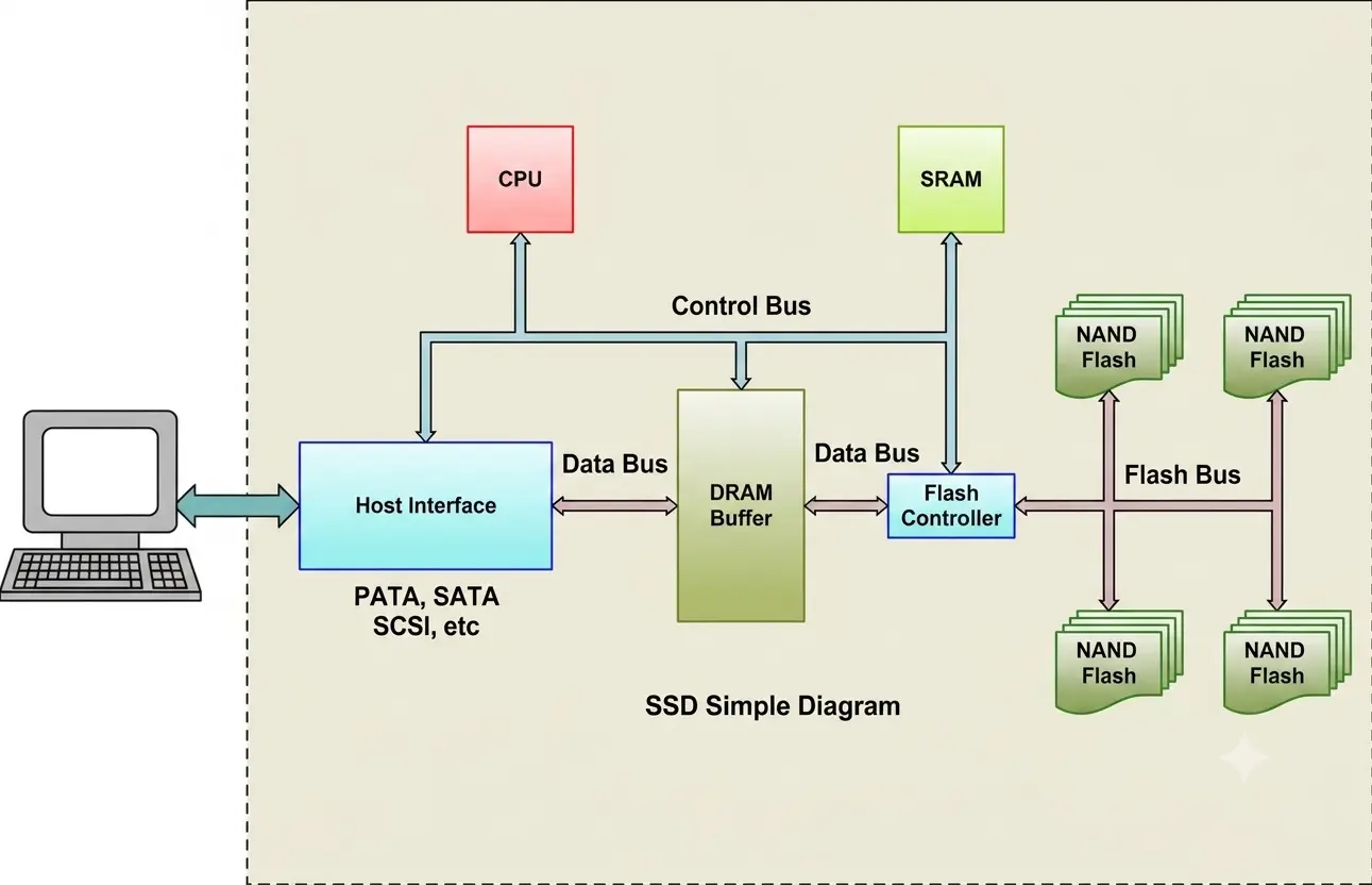
In direct mapping physical address is divided into three parts i.e., Tag bits, Cache Line Number and Byte offset.
Tag Number of Cache Lines/Index bit Offset Bit Given:-
Cache size: 16 KB
Block size: 4 words
Word size: 4 bytes (assuming a typical 32-bit architecture where each word is 4 bytes)
Address size: 32 bits
Calculate the Block Size in Bytes:
Since each block contains 4 words and each word is 4 bytes:
Block size = \( 4 \text{ words} \times 4 \text{ bytes/word} = 16 = 2^4 \text{ bytes} \)
Number of offset bits = \( \log_2 2^4 \) = 4 bits
Calculate the Number of Cache Blocks:
Block size = Line size = \( 2^4 \text{ bytes} \)
The total cache size is 16 KB = \( 2^{14} \text{ bytes} \) [ 1 KB = 210B]
Number of Lines = \( \frac{\text{Total cache size}}{\text{Line size}} = \frac{2^{14}}{2^4} = 2^{10} \text{ lines} \)
Number of Lines in the cache:
Number of index bits = \( \log_2 \text{(Number of lines)} = \log_2 2^{10} = \) 10 bits
Number of tag bits = Total Address bit − (Index bits + Offset bits) = \( 32 – (10 + 4) = \) 18 bits.