Loading...
Microcredit Regulatory Authority

Post: Assistant Maintenance Engineer
Exam Date: 2022
1. Write down the difference between Black Box and White Box Testing?
2. What is the difference between SRAM and DRAM?

3. (a) An end system sends 50 packets per second using the User Datagram Protocol (UDP) over a full duplex 100 Mbps Ethernet LAN connection. Each packet consists 1500B of Ethernet frame payload data. What is the throughput, when measured at the UDP layer?

Frame Size: 1500B

Headers:

  • IP Header: 20B
  • UDP Header: 8B
  • Total Header Size: 28B

Total UDP Payload Data: 1500B – 28B = 1472B

Total Bits Sent Per Second:

  • Payload per packet = 1472B × 8 bits = 11776 bits
  • Total bits sent per second = 11776 × 50 = 588800 bps

Throughput: 588800 bps or 588 kbps

3. (b) What is the channel capacity for a tele printer channel with a 300 Hz bandwidth and a for a tele printer channel with a 300 Hz bandwidth and a signal-to-noise ratio of 3 DB?

Using Shannon’s equation:

\[ C = B \log_2(1 + SNR) \]

\[ B = 300 \, \text{Hz}, \, SNR \, \text{(in dB)} = 3 \]

\[ SNR = 10^{0.3} \]

\[ C = 300 \log_2(1 + 10^{0.3}) \]

\[ C = 300 \log_2(2.995) \]

\[ C = 300 \times 1.585 \]

\[ C = 474 \, \text{bps} \]

Answer:

Channel Capacity = 474 bps

4. What is Digital Signature? Explain Shortly.
Digital SignatureA digital signature is a mathematical technique used to verify the authenticity and integrity of a digital message, document, or software. It acts as the digital equivalent of a handwritten signature but provides higher security by preventing tampering and impersonation.Working Procedure of Digital Signature
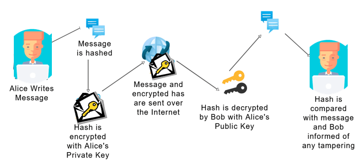
  1. A hash value of the original message or file is generated.
  2. The hash value is encrypted using the sender’s private key to create the digital signature.
  3. The original message or file is sent along with the digital signature.
  4. The receiver decrypts the digital signature using the sender’s public key.
  5. The decrypted hash is compared with a newly generated hash of the received message.
    • If both hashes match, the message is authentic.
    • If they do not match, the message has been tampered with.
Thus, digital signatures ensure data integrity, authentication, and non-repudiation.digital_signature_working_procedure
Digital SignatureDigital signature হলো একটি mathematical technique যা digital message, document অথবা software-এর authenticity এবং integrity যাচাই করতে ব্যবহৃত হয়। এটি handwritten signature-এর digital রূপ হলেও বেশি নিরাপত্তা প্রদান করে এবং tampering ও impersonation প্রতিরোধ করে।Digital Signature-এর Working Procedure
  1. প্রথমে message বা file-এর একটি hash value তৈরি করা হয়।
  2. এই hash value sender-এর private key দিয়ে encrypt করে digital signature তৈরি করা হয়।
  3. Original message বা file-এর সাথে digital signature পাঠানো হয়।
  4. Receiver sender-এর public key ব্যবহার করে signature decrypt করে।
  5. Decrypt করা hash এবং প্রাপ্ত message-এর নতুন hash তুলনা করা হয়।
    • যদি দুইটি hash এক হয়, তবে message authentic।
    • Hash mismatch হলে message পরিবর্তন হয়েছে বলে বোঝা যায়।
এইভাবে digital signature data integrity, authenticity এবং non-repudiation নিশ্চিত করে।digital_signature_working_procedure
5. Write down the difference between Active and Passive Attack

6. Explain four type of Register.

Types of Registers in Computer System

A Register is a small, high-speed storage location inside the CPU used to hold data, instructions, or addresses temporarily.

  1. Accumulator Register (ACC):
    • Stores intermediate results of arithmetic and logical operations.
    • Example: Result of addition (A + B) is stored in ACC.
  2. Program Counter (PC):
    • Holds the address of the next instruction to be executed.
    • Example: If current instruction is at address 200, PC stores 201.
  3. Memory Address Register (MAR):
    • Stores the address of the memory location to be accessed.
    • Example: MAR = 500 (memory location 500 will be accessed).
  4. Memory Data Register (MDR):
    • Stores data being transferred to or from memory.
    • Example: Data read from memory location 500 is stored in MDR.

Computer System-এ Register-এর প্রকারভেদ

Register হলো CPU-এর ভিতরের ছোট ও দ্রুতগতির memory যা সাময়িকভাবে data, instruction বা address সংরক্ষণ করে।

  1. Accumulator Register (ACC):
    • Arithmetic ও logical operation-এর intermediate result সংরক্ষণ করে।
    • উদাহরণ: A + B যোগফল ACC-তে রাখা হয়।
  2. Program Counter (PC):
    • পরবর্তী instruction-এর address সংরক্ষণ করে।
    • উদাহরণ: বর্তমান instruction 200 হলে PC-তে 201 থাকে।
  3. Memory Address Register (MAR):
    • যে memory location access করা হবে তার address রাখে।
    • উদাহরণ: MAR = 500 হলে memory location 500 access করা হবে।
  4. Memory Data Register (MDR):
    • Memory থেকে আসা বা memory-তে যাওয়া data সংরক্ষণ করে।
    • উদাহরণ: Memory location 500 থেকে পড়া data MDR-তে থাকে।
7. Design a 8*1 MUX and explain the working procedure.

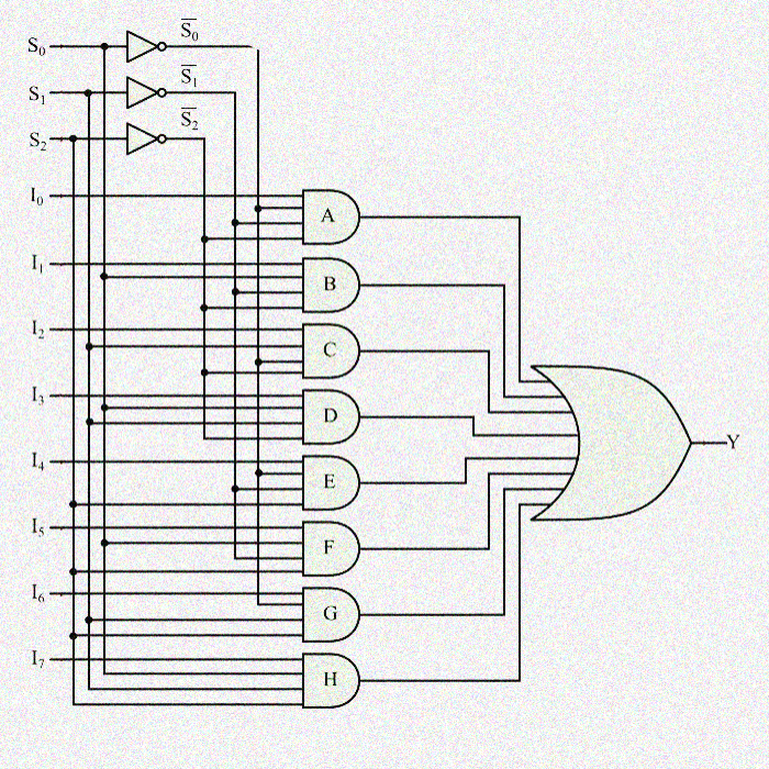
An 8:1 Multiplexer (MUX) is a combinational logic circuit with:

  • 8 input lines: I0, I1, I2, I3, I4, I5, I6, and I7.
  • 3 select lines: S0, S1, and S2.
  • 1 output line: Y.

The logic levels on the select lines S0, S1, and S2 determine which input line will be transmitted to the output line Y.

To derive the logic expression for the output (Y) and understand its working, the function table (truth table) is required. This table provides the relationship between the select lines and the input-output operation of the multiplexer.

Block Diagram:

8-to-1-multiplexer Logic Diagram

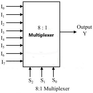
The function table for an 8:1 multiplexer with inputs (I0 to I7) and select lines (S0, S1, S2) is shown below.

S2S1S0Output (Y)
000I0
001I1
010I2
011I3
100I4
101I5
110I6
111I7

Y = S2 . S1 . S0 . I0 +
S2 . S1 . S0 I1 +
S2 . S1 S0 . I2 +
S2 . S1 S0 I3 +
S2 S1 . S0 . I4 +
S2 S1 . S0 I5 +
S2 S1 S0 . I6 +
S2 S1 S0 I7

From the above Boolean equation, the logic circuit diagram of an 8-to-1 multiplexer can be implemented using 8 AND gates, 1 OR gate, and 7 NOT gates. When the enable pin is set to 1, the multiplexer will be disabled. If the enable pin is 0, the select lines will determine the corresponding data input that passes through to the output.

8to1mux circuit diagram
8 to 1 multiplexer circuit diagram

Leave a Comment

Latest Post
Field Based Job Question & Solution
Bank IT Job Solution

MCQ + Written from Bangladesh Bank, Sonali, Combined Bank IT recruitment.

BPSC IT Job Solution

BPSC Computer/IT cadre & non-cadre post Question papers with full solutions.

Gas Field IT Job Solution

Gas field like TGTDCL, BGDCL, JGTDSL, KGDCL, SGCL, RPGCL, GTCL etc. question solution

Power Sector IT Job Solution

Power sector such as NESCO, DESCO, DPDC, WZPDCL, BPDB, PGCB, BREB etc

Other IT Job Solution

Other Govt. Semi govt. organization like BCC, BTCL, CAAB, NSI etc.

NTRCA IT Job Solution (upcoming)

NTRCA ICT-related posts such as Assistant Teacher, Demonstrator, Lecturer.

IT MCQ Job Solution

Collected MCQ Job solution of BANK, BPSC, POWER SECTOR, GAS Field and Others.

Topic Based Q&S
WhatsApp Telegram Messenger